

source:Industry News release time:2021-09-13 Article author:sznbone Popular:pcb
The so-called circuit board gold finger refers to a row of equidistantly arranged square pads, exposed copper and gold-plated. It is mostly used for electrical connection pins for board cards, LCD connections, motherboards, chassis, etc., because the copper foil nickel-plated layer is plated with a thin layer of gold.
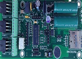
One, the definition and function of the gold finger of the PCB circuit board:
Golden Finger: (GoldFinger or EdgeConnector) Insert one end of the PCB circuit board into the connector card slot, and use the connector pin as the outlet of the circuit board to connect to the outside, so that the pad or copper skin is in contact with the pin at the corresponding position. To achieve the purpose of conduction, and plate this pad or copper on the PCB board with nickel and gold, because it is in the shape of a finger, it is called a gold finger. The reason why gold is selected is because of its superior conductivity and oxidation resistance. .But because of the extremely high cost of gold, it is only used for partial gilding such as gold fingers.
Double-sided circuit board gold finger plus plating hole filling
Two, circuit board gold finger classification and identification characteristics
The gold finger classification of the circuit board:
1. Conventional gold finger (flush finger);
2. Segmented cheats (intermittent cheats);
3. Long and short golden fingers (ie uneven golden fingers).
Gold finger circuit boards of different lengths
1. Conventional gold fingers (flush fingers): rectangular pads with the same length and width are arranged neatly at the edge of the board. The picture below shows: network cards, graphics cards and other types of physical objects, with more gold fingers. Some small boards have fewer gold fingers ;
2. Segmented golden fingers (intermittent golden fingers): rectangular pads with different lengths located on the edge of the board, and the front section is disconnected;
3. Long and short golden fingers (ie uneven golden fingers): rectangular pads with different lengths located on the edge of the board.
PCB circuit board gold finger
Features: No character frame and marking, conventional solder mask opening window. Most shapes have grooves. The gold fingers protrude from the edge of the board, or are close to the edge of the board. Some boards have gold fingers at both ends. Normal gold fingers are on both sides Yes, some PCB circuit boards have only single-sided gold fingers. Some circuit boards have a wide single gold finger.
Read recommendations:
Six-layer Immersion Gold Board (BGA)
Desoldering skills and daily problems of PCBA processing.Electronic assembly PCB
Popular recommended products
Six-layer Immersion Gold Board (BGA)
2021-05-24Six-layer Immersion Gold Board (BGA)
2021-04-27High frequency PCB
2021-04-27High frequency PCB
2021-04-27Single-sided double-layer AL base PCB
2021-04-27Aluminum substrate (double-sided)
2021-04-27Six-layer Immersion Gold Board (BGA)
2021-05-27High frequency PCB
2021-04-27Laminate copper-based PCB after 4L (sample)
2021-04-27Single copper base PCB
2021-04-27Mobile phone template (six layers)
2021-04-27Six-layer Immersion Gold Board (BGA)
2021-05-24Computer card board (four layers)
2021-04-25Six-layer Immersion Gold Board (BGA)
2021-05-27Six-layer Immersion Gold Board (BGA)
2021-05-27Six-layer Immersion Gold Board (BGA)
2021-04-27Six-layer Immersion Gold Board (BGA)
2021-04-27High frequency PCB
2021-04-27Six-layer Immersion Gold Board (BGA)
2021-04-27Display board (six layers)
2021-04-27Network communication board (sixth floor)
2021-04-29Six-layer Immersion Gold Board (BGA)
2021-05-27Silver oil perforated plate (double-sided)
2021-04-27SMT stickers
2021-05-27Six-layer Immersion Gold Board (BGA)
2021-04-26Six-layer Immersion Gold Board (BGA)
2021-04-26Six-layer Immersion Gold Board (BGA)
2021-04-26DIP plugin
2021-05-27Mobile phone board
2021-05-27Six-layer Immersion Gold Board (BGA)
2021-04-26SMT stickers
2021-05-27Six-layer Immersion Gold Board (BGA)
2021-04-26Mobile phone board
2021-04-27DIP plugin
2021-05-27Related Information
The relationship between PCB safety distance and voltage
2024-04-22SMT surface mount processing.Hybrid circuit board PCB
2024-04-15PCB enterprises should pay attention to SMT matters.Electronic components PCB
2024-04-03PCB - the core building block of electronic products.Automotive Electronics PCB
2024-03-25PCB - the bridge and link of the electronic world
2024-03-18How to define high-frequency and high-precision circuit boards.Industrial Electronics PCB
2024-03-11USB PCB interface layout and wiring requirements
2024-01-22Electrolytic capacitor PCB.Steps for using PCB pins
2024-01-15Automotive ElectronicWhat aspects should be considered when processing and manufacturing PCB boards?
2024-01-08Electrolytic capaciWhat is the difference between a gold-plated circuit board and a gold-plated one?
2023-12-25When grinding PCB boards, attention should be paid to.Oscillator (belonging to crystal) PCB
2023-12-18Industrial Electronics PCB!What precautions should be taken when copying and grinding PCB boards
2023-12-11Do you know who is more suitable for LED direct display, regarding the difference between PCB board
2023-12-05Aluminum electrolytic capacitor PCB.What are the standards for selecting PCB boards
2023-11-27Surface Mount Technology (SMT) Phase PCB
2023-11-20Oscillator (belonging to crystal) PCB.The main functions of PCB board
2023-11-13What is the difference between RO filter and PCB filter
2023-11-06Method for determining blind hole PCB board
2023-11-01Electronic Manufacturing Services PCB!What are the effects of PCB board color on performance?
2023-10-23Introduction to the Manufacturing Steps and Requirements of PCBA Test Stand
2023-10-16PCB version maturity stage.AOI circuit board price
2023-09-25How to maintain a PCB circuit board
2023-09-19Development Trend of Printed Circuit Board.Zener diode PCB Vendor
2023-09-14Common problems and cause analysis of PCB circuit board sampling.Zener diode PCB price
2023-09-08What are the issues that need to be understood in PCB circuit board design?IGBT module PCB factory
2023-09-08How to reduce the risk of bending and deformation in PCB circuit board production?Inverter PCB Produ
2023-08-16What are the three main factors that constitute welding defects in PCB circuit boards?Multilayer PCB
2023-08-16The structure of a glass teapot.LCD Module PCB factory
2023-08-11Glass teapot.Inverter PCB Processing
2023-08-11PCB online debugging
2023-08-08
CopyRight © 2007-2024Shenzhen Weienchen Technology Co., Ltd.
粤ICP备2021061255号

Address:
1205, Floor 12, Building 3, Chuangyi Office Building, No. 110, Ziheng West Road, Jinsha Community, Kengzi Street, Pingshan District, Shenzhen, Guangdong, China

Tel:
+86-755-29662580

Email:
sales@victoriapcb.com

PCB

PCBA
Service
Process
 Tel: +86-755-29662580
 Email: sales@victoriapcb.com
 中
中 current position:


