

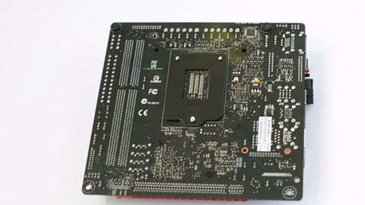
source:Industry News release time:2022-05-13 Article author:yu Popular:pcb
General HDI circuit boards use metallized blind holes to connect each circuit layer that needs to be connected. The diameter is generally not greater than 0.2_; then the dielectric layer under the blind hole is removed by a laser ablation process to form a blind hole reaching the upper copper foil layer; then, the blind hole is metallized to realize the two layers of copper foil. Interconnection; then, you can continue to laminate the build-up layer, and use the same method to make metallized blind holes after the build-up layer and use the same method to make metallized blind holes after the build-up layer to realize the interconnection between other layers.
The method for making blind holes on an HDI circuit board includes the following steps: ①coating photosensitive epoxy resin; ②baking the circuit board and curing the resin; The epoxy resin at the hole position makes the copper pad of the inner layer pattern prominent; ④ mechanically drill through holes; ⑤ metallization plating; ⑥ chemical etching copper.
How to define SMD is the first difficulty in CAM production.
In the PCB production process, factors such as pattern transfer and etching will affect the final pattern, so we need to compensate the lines and SMD separately in the CAM production according to the customer's acceptance criteria. If we do not define the SMD correctly, the finished product may appear partially SMD is too small.
Specific production steps:
1. Close the drilling layer corresponding to blind holes and buried holes.
2. Define SMD
3. Use the FeaturesFilterpopup and Referenceselectionpopup functions to find the pads that include blind holes from the top layer and bottom layer, movetot layer and b layer respectively.
4. Use the Referenceselectionpopup function on the t layer (the layer where the CSP pads are located) to select and delete the 0.3mm pad that touches the blind hole, and delete the 0.3mm pad in the CSP area of the top layer. Then design the size, position and number of CSP pads according to the customer, make a CSP and define it as SMD, then copy the CSP pads to the TOP layer, and add the pads corresponding to the blind holes on the TOP layer. The b layer is made in a similar way.
5. Find out other missing or multi-defined SMDs according to the network file provided by the customer.
Plugs and Solder Mask:
In the HDI lamination configuration, the secondary outer layer is generally made of RCC material, which has a thin dielectric thickness and a small amount of glue. The process experimental data shows that if the thickness of the finished product is greater than 0.8mm, the metallization groove is greater than or equal to 0.8mmX2.0mm , the metallized hole is greater than or equal to 1.2mm, and two sets of plug hole files must be made. That is, the holes are plugged twice, the inner layer is leveled with resin, and the outer layer is directly plugged with solder mask ink before solder mask. During the solder mask fabrication process, vias often fall on or next to the SMD. The customer requires all vias to be plugged, so the vias with exposed or exposed half of the holes are prone to oil leakage during solder mask exposure.
Read recommendations:
Popular recommended products
Silver oil perforated plate (double-sided)
2021-04-27Six-layer Immersion Gold Board (BGA)
2021-04-27Network communication board (sixth floor)
2021-04-29Six-layer Immersion Gold Board (BGA)
2021-05-27Aluminum substrate (double-sided)
2021-04-27Six-layer Immersion Gold Board (BGA)
2021-04-27Laminate copper-based PCB after 4L (sample)
2021-04-27Six-layer Immersion Gold Board (BGA)
2021-05-27Single-sided double-layer AL base PCB
2021-04-27Computer card board (four layers)
2021-04-25High frequency PCB
2021-04-27Six-layer Immersion Gold Board (BGA)
2021-05-27High frequency PCB
2021-04-27Six-layer Immersion Gold Board (BGA)
2021-04-27Six-layer Immersion Gold Board (BGA)
2021-04-27Six-layer Immersion Gold Board (BGA)
2021-05-24High frequency PCB
2021-04-27Mobile phone template (six layers)
2021-04-27Display board (six layers)
2021-04-27High frequency PCB
2021-04-27Single copper base PCB
2021-04-27Six-layer Immersion Gold Board (BGA)
2021-05-24Six-layer Immersion Gold Board (BGA)
2021-05-27DIP plugin
2021-05-27Mobile phone board
2021-04-27SMT stickers
2021-05-27Six-layer Immersion Gold Board (BGA)
2021-04-26DIP plugin
2021-05-27Six-layer Immersion Gold Board (BGA)
2021-04-26Six-layer Immersion Gold Board (BGA)
2021-04-26Six-layer Immersion Gold Board (BGA)
2021-04-26Mobile phone board
2021-05-27Six-layer Immersion Gold Board (BGA)
2021-04-26SMT stickers
2021-05-27Related Information
Multilayer Printed Circuit Board.What is the eq of PCB
2024-05-20The relationship between PCB safety distance and voltage
2024-04-22SMT surface mount processing.Hybrid circuit board PCB
2024-04-15PCB enterprises should pay attention to SMT matters.Electronic components PCB
2024-04-03PCB - the core building block of electronic products.Automotive Electronics PCB
2024-03-25PCB - the bridge and link of the electronic world
2024-03-18How to define high-frequency and high-precision circuit boards.Industrial Electronics PCB
2024-03-11USB PCB interface layout and wiring requirements
2024-01-22Electrolytic capacitor PCB.Steps for using PCB pins
2024-01-15Automotive ElectronicWhat aspects should be considered when processing and manufacturing PCB boards?
2024-01-08Electrolytic capaciWhat is the difference between a gold-plated circuit board and a gold-plated one?
2023-12-25When grinding PCB boards, attention should be paid to.Oscillator (belonging to crystal) PCB
2023-12-18Industrial Electronics PCB!What precautions should be taken when copying and grinding PCB boards
2023-12-11Do you know who is more suitable for LED direct display, regarding the difference between PCB board
2023-12-05Aluminum electrolytic capacitor PCB.What are the standards for selecting PCB boards
2023-11-27Surface Mount Technology (SMT) Phase PCB
2023-11-20Oscillator (belonging to crystal) PCB.The main functions of PCB board
2023-11-13What is the difference between RO filter and PCB filter
2023-11-06Method for determining blind hole PCB board
2023-11-01Electronic Manufacturing Services PCB!What are the effects of PCB board color on performance?
2023-10-23Introduction to the Manufacturing Steps and Requirements of PCBA Test Stand
2023-10-16PCB version maturity stage.AOI circuit board price
2023-09-25How to maintain a PCB circuit board
2023-09-19Development Trend of Printed Circuit Board.Zener diode PCB Vendor
2023-09-14Common problems and cause analysis of PCB circuit board sampling.Zener diode PCB price
2023-09-08What are the issues that need to be understood in PCB circuit board design?IGBT module PCB factory
2023-09-08How to reduce the risk of bending and deformation in PCB circuit board production?Inverter PCB Produ
2023-08-16What are the three main factors that constitute welding defects in PCB circuit boards?Multilayer PCB
2023-08-16The structure of a glass teapot.LCD Module PCB factory
2023-08-11Glass teapot.Inverter PCB Processing
2023-08-11
CopyRight © 2007-2024Shenzhen Weienchen Technology Co., Ltd.
粤ICP备2021061255号

Address:
1205, Floor 12, Building 3, Chuangyi Office Building, No. 110, Ziheng West Road, Jinsha Community, Kengzi Street, Pingshan District, Shenzhen, Guangdong, China

Tel:
+86-755-29662580

Email:
sales@victoriapcb.com

PCB

PCBA
Service
Process
 Tel: +86-755-29662580
 Email: sales@victoriapcb.com
 中
中 current position:


