

source:Industry News release time:2022-06-21 Article author:yu Popular:pcb
The warpage of the PCB long board/strip board has a great influence on the production of the printed circuit board, and warpage is also one of the important problems in the production process of the PCB long board/strip board. The long board is bent after welding, and the component feet are difficult to align. The PCB long board/strip board cannot be installed on the chassis or the socket in the machine, so the warpage of the circuit board will affect the normal operation of the entire subsequent process. At this stage, the printed circuit board has entered the era of surface mounting and chip mounting, and the requirements for the warpage of the circuit board are getting higher and higher. So we have to find the reason for the warping of the halfway gang.
1. Engineering design: Matters needing attention in the design of PCB long board/strip board: A. The arrangement of the prepreg between layers should be symmetrical, such as a six-layer circuit board, the thickness between 1-2 and 5-6 layers and the number of sheets of prepreg It should be consistent, otherwise it will warp easily after lamination. B. Multilayer circuit board core board and prepreg should use the same supplier's products. C. The area of the circuit pattern on the A side and the B side of the outer layer should be as close as possible. If the A side is a large copper surface, and the B side only has a few lines, this kind of printed circuit board is easy to warp after etching. If the line area on the two sides is too different, you can add some independent grids on the thin side for balance.
2. Baking the board before cutting: The purpose of baking the board before cutting the copper clad laminate (150 degrees Celsius, time 8±2 hours) is to remove the moisture in the board, and at the same time, the resin in the board is completely cured, and the remaining stress in the board is further eliminated. This is helpful in preventing board warping. At present, many double-sided and multi-layer boards still insist on the step of baking the board before or after cutting. However, there are some exceptions for board factories. At present, the time requirements for PCB long board/strip board baking are also inconsistent, ranging from 4 to 10 hours. Decide. Baking after cutting into a jigsaw or drying the whole piece of aniseed before unloading, both methods are feasible, it is recommended to bake the board after cutting. The inner board should also be baked.
Read recommendations:
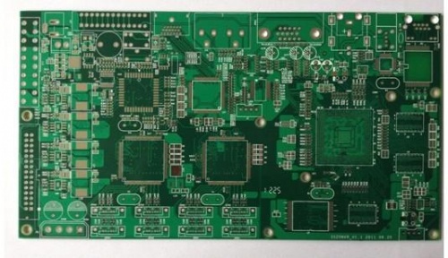
Six-layer Immersion Gold Board (BGA)
Mobile phone template (six layers)
Six-layer Immersion Gold Board (BGA)
Analysis of the key points of current and voltage feedback judgment.Industrial Electronics PCB Whole
Popular recommended products
Silver oil perforated plate (double-sided)
2021-04-27Six-layer Immersion Gold Board (BGA)
2021-04-27Computer card board (four layers)
2021-04-25Six-layer Immersion Gold Board (BGA)
2021-05-27High frequency PCB
2021-04-27Six-layer Immersion Gold Board (BGA)
2021-05-27Six-layer Immersion Gold Board (BGA)
2021-04-27Six-layer Immersion Gold Board (BGA)
2021-05-24Six-layer Immersion Gold Board (BGA)
2021-05-27Six-layer Immersion Gold Board (BGA)
2021-05-24Aluminum substrate (double-sided)
2021-04-27Six-layer Immersion Gold Board (BGA)
2021-04-27Single-sided double-layer AL base PCB
2021-04-27High frequency PCB
2021-04-27Display board (six layers)
2021-04-27Single copper base PCB
2021-04-27Laminate copper-based PCB after 4L (sample)
2021-04-27High frequency PCB
2021-04-27Six-layer Immersion Gold Board (BGA)
2021-04-27High frequency PCB
2021-04-27Network communication board (sixth floor)
2021-04-29Six-layer Immersion Gold Board (BGA)
2021-05-27Mobile phone template (six layers)
2021-04-27SMT stickers
2021-05-27Six-layer Immersion Gold Board (BGA)
2021-04-26Six-layer Immersion Gold Board (BGA)
2021-04-26Mobile phone board
2021-04-27Six-layer Immersion Gold Board (BGA)
2021-04-26Six-layer Immersion Gold Board (BGA)
2021-04-26DIP plugin
2021-05-27DIP plugin
2021-05-27Six-layer Immersion Gold Board (BGA)
2021-04-26Mobile phone board
2021-05-27SMT stickers
2021-05-27Related Information
The relationship between PCB safety distance and voltage
2024-04-22SMT surface mount processing.Hybrid circuit board PCB
2024-04-15PCB enterprises should pay attention to SMT matters.Electronic components PCB
2024-04-03PCB - the core building block of electronic products.Automotive Electronics PCB
2024-03-25PCB - the bridge and link of the electronic world
2024-03-18How to define high-frequency and high-precision circuit boards.Industrial Electronics PCB
2024-03-11USB PCB interface layout and wiring requirements
2024-01-22Electrolytic capacitor PCB.Steps for using PCB pins
2024-01-15Automotive ElectronicWhat aspects should be considered when processing and manufacturing PCB boards?
2024-01-08Electrolytic capaciWhat is the difference between a gold-plated circuit board and a gold-plated one?
2023-12-25When grinding PCB boards, attention should be paid to.Oscillator (belonging to crystal) PCB
2023-12-18Industrial Electronics PCB!What precautions should be taken when copying and grinding PCB boards
2023-12-11Do you know who is more suitable for LED direct display, regarding the difference between PCB board
2023-12-05Aluminum electrolytic capacitor PCB.What are the standards for selecting PCB boards
2023-11-27Surface Mount Technology (SMT) Phase PCB
2023-11-20Oscillator (belonging to crystal) PCB.The main functions of PCB board
2023-11-13What is the difference between RO filter and PCB filter
2023-11-06Method for determining blind hole PCB board
2023-11-01Electronic Manufacturing Services PCB!What are the effects of PCB board color on performance?
2023-10-23Introduction to the Manufacturing Steps and Requirements of PCBA Test Stand
2023-10-16PCB version maturity stage.AOI circuit board price
2023-09-25How to maintain a PCB circuit board
2023-09-19Development Trend of Printed Circuit Board.Zener diode PCB Vendor
2023-09-14Common problems and cause analysis of PCB circuit board sampling.Zener diode PCB price
2023-09-08What are the issues that need to be understood in PCB circuit board design?IGBT module PCB factory
2023-09-08How to reduce the risk of bending and deformation in PCB circuit board production?Inverter PCB Produ
2023-08-16What are the three main factors that constitute welding defects in PCB circuit boards?Multilayer PCB
2023-08-16The structure of a glass teapot.LCD Module PCB factory
2023-08-11Glass teapot.Inverter PCB Processing
2023-08-11PCB online debugging
2023-08-08
CopyRight © 2007-2024Shenzhen Weienchen Technology Co., Ltd.
粤ICP备2021061255号

Address:
1205, Floor 12, Building 3, Chuangyi Office Building, No. 110, Ziheng West Road, Jinsha Community, Kengzi Street, Pingshan District, Shenzhen, Guangdong, China

Tel:
+86-755-29662580

Email:
sales@victoriapcb.com

PCB

PCBA
Service
Process
 Tel: +86-755-29662580
 Email: sales@victoriapcb.com
 中
中 current position:


