source:Industry News release time:2023-04-07 Article author:yu Popular:pcb

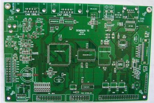
When the PCB is encapsulated in PCB, the problem of poor grasping the pads often encounters the problem of poor grasping pads, because the information we consider is the size of the component itself, such as the width of the pin, the spacing, etc., but on the PCB board, but on the PCB board, etc. The corresponding pads should be slightly larger than the size of the pin, otherwise the reliability of welding will not be guaranteed. The following will mainly talk about the norms of the pad size.
In order to ensure the welding quality of the patch component (SMT), when designing the SMT printing board, except for the printed board, the 3mm-8mm process should be left out. In addition to the distance between the orientation of the meta component and the distance between the adjacent components, we believe that we should pay special attention to the following points:
(1) On the printed board, any of the conductive graphics (such as interconnection, grounding, interoperability panel, etc.) and the copper foil that are required should be nude copper foil. That is, the metal coating that is not allowed to be plated than the welding temperature, such as tin lead alloys, etc., to avoid causing the welding membrane at the coating layer to break or wrinkle to ensure the welding and appearance of the PCB board.
(2) When checking or calling the graphic size data of the pad, it should be matched with the size of the encapsulated shape, solder end, pins, etc. of the components you selected. It is necessary to overcome the bad habits of the graphic size of the pad in the software library that you see without analysis or control or call. When designing, selected or calling the graphic size of the pad, you should also distinguish the components you chose, its code (such as chip resistance, capacitance) and welding -related dimensions (such as SOIC, QFP, etc.).
(3) The welding reliability of the surface -sticker component depends mainly on the length of the pad rather than width.
(A) As shown in Figure 1, the length B of the pads is equal to the length T of the weld (or pin), plus the extension length B1 of the inner side (pad) of the weld (or pin) (Or pins) extension length B2, which is B = T+B1+B2. Among them, the length of B1 (about 0.05mm -0.6mm) should not only benefit the welding joints that can form a good moon -shaped outline when welded melting, but also to avoid the phenomenon of bridge and the installation deviation of the components. ; The length of B2 (about 0.25mm -1.5mm), mainly to ensure that the best welding joints that can form the best moon -shaped outline are advocated (for SOIC, QFP and other devices, it should also take into account the ability of its pads to resist and peeling).)
Read recommendations:
Computer card board (four layers)
Single-sided double-layer AL base PCB
Popular recommended products
Six-layer Immersion Gold Board (BGA)
2021-05-27Six-layer Immersion Gold Board (BGA)
2021-05-27Six-layer Immersion Gold Board (BGA)
2021-05-27Six-layer Immersion Gold Board (BGA)
2021-04-27Single-sided double-layer AL base PCB
2021-04-27Computer card board (four layers)
2021-04-25Display board (six layers)
2021-04-27Network communication board (sixth floor)
2021-04-29Laminate copper-based PCB after 4L (sample)
2021-04-27Mobile phone template (six layers)
2021-04-27Aluminum substrate (double-sided)
2021-04-27Six-layer Immersion Gold Board (BGA)
2021-05-27High frequency PCB
2021-04-27Six-layer Immersion Gold Board (BGA)
2021-04-27Single copper base PCB
2021-04-27Six-layer Immersion Gold Board (BGA)
2021-04-27High frequency PCB
2021-04-27Silver oil perforated plate (double-sided)
2021-04-27High frequency PCB
2021-04-27Six-layer Immersion Gold Board (BGA)
2021-05-24Six-layer Immersion Gold Board (BGA)
2021-04-27Six-layer Immersion Gold Board (BGA)
2021-05-24High frequency PCB
2021-04-27DIP plugin
2021-05-27Mobile phone board
2021-04-27Six-layer Immersion Gold Board (BGA)
2021-04-26Six-layer Immersion Gold Board (BGA)
2021-04-26Six-layer Immersion Gold Board (BGA)
2021-04-26Six-layer Immersion Gold Board (BGA)
2021-04-26SMT stickers
2021-05-27Six-layer Immersion Gold Board (BGA)
2021-04-26SMT stickers
2021-05-27DIP plugin
2021-05-27Mobile phone board
2021-05-27Related Information
The relationship between PCB safety distance and voltage
2024-04-22SMT surface mount processing.Hybrid circuit board PCB
2024-04-15PCB enterprises should pay attention to SMT matters.Electronic components PCB
2024-04-03PCB - the core building block of electronic products.Automotive Electronics PCB
2024-03-25PCB - the bridge and link of the electronic world
2024-03-18How to define high-frequency and high-precision circuit boards.Industrial Electronics PCB
2024-03-11USB PCB interface layout and wiring requirements
2024-01-22Electrolytic capacitor PCB.Steps for using PCB pins
2024-01-15Automotive ElectronicWhat aspects should be considered when processing and manufacturing PCB boards?
2024-01-08Electrolytic capaciWhat is the difference between a gold-plated circuit board and a gold-plated one?
2023-12-25When grinding PCB boards, attention should be paid to.Oscillator (belonging to crystal) PCB
2023-12-18Industrial Electronics PCB!What precautions should be taken when copying and grinding PCB boards
2023-12-11Do you know who is more suitable for LED direct display, regarding the difference between PCB board
2023-12-05Aluminum electrolytic capacitor PCB.What are the standards for selecting PCB boards
2023-11-27Surface Mount Technology (SMT) Phase PCB
2023-11-20Oscillator (belonging to crystal) PCB.The main functions of PCB board
2023-11-13What is the difference between RO filter and PCB filter
2023-11-06Method for determining blind hole PCB board
2023-11-01Electronic Manufacturing Services PCB!What are the effects of PCB board color on performance?
2023-10-23Introduction to the Manufacturing Steps and Requirements of PCBA Test Stand
2023-10-16PCB version maturity stage.AOI circuit board price
2023-09-25How to maintain a PCB circuit board
2023-09-19Development Trend of Printed Circuit Board.Zener diode PCB Vendor
2023-09-14Common problems and cause analysis of PCB circuit board sampling.Zener diode PCB price
2023-09-08What are the issues that need to be understood in PCB circuit board design?IGBT module PCB factory
2023-09-08How to reduce the risk of bending and deformation in PCB circuit board production?Inverter PCB Produ
2023-08-16What are the three main factors that constitute welding defects in PCB circuit boards?Multilayer PCB
2023-08-16The structure of a glass teapot.LCD Module PCB factory
2023-08-11Glass teapot.Inverter PCB Processing
2023-08-11PCB online debugging
2023-08-08