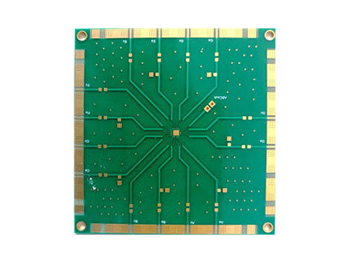
source:Industry News release time:2022-10-09 Article author:yu Popular:pcb

1. Record PCB related details
Get a PCB, first record the models, parameters, and positions of all components on the paper, especially the direction of diodes, triodes, and the direction of IC notch. It is best to take two pictures of the component locations with a digital camera. Many pcb circuit boards are getting more and more advanced, and some of the diodes and triodes above are not visible at all.
2. Scanned image
Remove all components and remove the tin from the PAD holes. Clean the PCB with alcohol, and then put it into the scanner. When the scanner scans, you need to slightly increase the scanned pixels to get a clearer image.
Then lightly polish the top and bottom layers with water gauze paper until the copper film is shiny, put it into the scanner, start PHOTOSHOP, and scan the two layers in color.
Note that the PCB must be placed horizontally and vertically in the scanner, otherwise the scanned image will not be available.
3. Adjust the corrected image
Adjust the contrast and brightness of the canvas to make the part with copper film and the part without copper film have a strong contrast, then turn the secondary image to black and white, check whether the lines are clear, if not, repeat this step. If it is clear, save the picture as TOP BMP and BOT BMP files in black and white BMP format. If there is any problem with the picture, you can also use PHOTOSHOP to repair and correct it.
4. Check the position coincidence of PAD and VIA
Convert the two BMP format files to PROTEL format files respectively, and transfer two layers in PROTEL. For example, the positions of PAD and VIA after the two layers are basically the same, indicating that the first few steps are well done. If there is any deviation, then Repeat step three. Therefore, PCB copying is a work that requires great patience, because a little problem will affect the quality and the matching degree after copying.
5. Drawing layers
Convert the BMP of the TOP layer to the TOP PCB, pay attention to convert it to the SILK layer, which is the yellow layer, and then you can trace the line on the TOP layer, and place the device according to the drawing in the second step. After painting, delete the SILK layer. Repeat until all layers are drawn.
6. Combined picture of TOP PCB and BOT PCB
Transfer the TOP PCB and BOT PCB in PROTEL and combine them into one picture.
7. Laser printing TOP LAYER, BOTTOM LAYER
Use a laser printer to print the TOP LAYER and BOTTOM LAYER on the transparent film (1:1 ratio), put the film on the PCB, and compare whether there is any error. If it is correct, you are done.
8. Test
Test whether the electronic performance of the copy board is the same as that of the original board. If so then it's really done.
Read recommendations:
Why do we need test points on the PCB circuit board?Electronic Manufacturing Services PCB
Popular recommended products
High frequency PCB
2021-04-27Six-layer Immersion Gold Board (BGA)
2021-05-24High frequency PCB
2021-04-27Single-sided double-layer AL base PCB
2021-04-27Silver oil perforated plate (double-sided)
2021-04-27Single copper base PCB
2021-04-27Six-layer Immersion Gold Board (BGA)
2021-05-27Six-layer Immersion Gold Board (BGA)
2021-05-27Six-layer Immersion Gold Board (BGA)
2021-05-27Six-layer Immersion Gold Board (BGA)
2021-04-27Six-layer Immersion Gold Board (BGA)
2021-05-24Six-layer Immersion Gold Board (BGA)
2021-05-27Six-layer Immersion Gold Board (BGA)
2021-04-27Display board (six layers)
2021-04-27Network communication board (sixth floor)
2021-04-29Computer card board (four layers)
2021-04-25Laminate copper-based PCB after 4L (sample)
2021-04-27High frequency PCB
2021-04-27Aluminum substrate (double-sided)
2021-04-27Mobile phone template (six layers)
2021-04-27Six-layer Immersion Gold Board (BGA)
2021-04-27Six-layer Immersion Gold Board (BGA)
2021-04-27High frequency PCB
2021-04-27Mobile phone board
2021-04-27Six-layer Immersion Gold Board (BGA)
2021-04-26Six-layer Immersion Gold Board (BGA)
2021-04-26SMT stickers
2021-05-27SMT stickers
2021-05-27DIP plugin
2021-05-27DIP plugin
2021-05-27Mobile phone board
2021-05-27Six-layer Immersion Gold Board (BGA)
2021-04-26Six-layer Immersion Gold Board (BGA)
2021-04-26Six-layer Immersion Gold Board (BGA)
2021-04-26Related Information
The relationship between PCB safety distance and voltage
2024-04-22SMT surface mount processing.Hybrid circuit board PCB
2024-04-15PCB enterprises should pay attention to SMT matters.Electronic components PCB
2024-04-03PCB - the core building block of electronic products.Automotive Electronics PCB
2024-03-25PCB - the bridge and link of the electronic world
2024-03-18How to define high-frequency and high-precision circuit boards.Industrial Electronics PCB
2024-03-11USB PCB interface layout and wiring requirements
2024-01-22Electrolytic capacitor PCB.Steps for using PCB pins
2024-01-15Automotive ElectronicWhat aspects should be considered when processing and manufacturing PCB boards?
2024-01-08Electrolytic capaciWhat is the difference between a gold-plated circuit board and a gold-plated one?
2023-12-25When grinding PCB boards, attention should be paid to.Oscillator (belonging to crystal) PCB
2023-12-18Industrial Electronics PCB!What precautions should be taken when copying and grinding PCB boards
2023-12-11Do you know who is more suitable for LED direct display, regarding the difference between PCB board
2023-12-05Aluminum electrolytic capacitor PCB.What are the standards for selecting PCB boards
2023-11-27Surface Mount Technology (SMT) Phase PCB
2023-11-20Oscillator (belonging to crystal) PCB.The main functions of PCB board
2023-11-13What is the difference between RO filter and PCB filter
2023-11-06Method for determining blind hole PCB board
2023-11-01Electronic Manufacturing Services PCB!What are the effects of PCB board color on performance?
2023-10-23Introduction to the Manufacturing Steps and Requirements of PCBA Test Stand
2023-10-16PCB version maturity stage.AOI circuit board price
2023-09-25How to maintain a PCB circuit board
2023-09-19Development Trend of Printed Circuit Board.Zener diode PCB Vendor
2023-09-14Common problems and cause analysis of PCB circuit board sampling.Zener diode PCB price
2023-09-08What are the issues that need to be understood in PCB circuit board design?IGBT module PCB factory
2023-09-08How to reduce the risk of bending and deformation in PCB circuit board production?Inverter PCB Produ
2023-08-16What are the three main factors that constitute welding defects in PCB circuit boards?Multilayer PCB
2023-08-16The structure of a glass teapot.LCD Module PCB factory
2023-08-11Glass teapot.Inverter PCB Processing
2023-08-11PCB online debugging
2023-08-08