

source:Industry News release time:2022-04-25 Article author:yu Popular:pcb
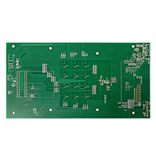
In the PCB circuit board industry, it is natural to set test points on the circuit board, but for newcomers who are new to PCB circuit boards, what are the test points? It is a question, so today, the editor of the PCB manufacturer will take you to understand why the test points should be set on the PCB circuit board.
Simply put, the purpose of setting test points is to test whether the components on the circuit board meet the specifications and solderability. For example, if you want to check whether there is any problem with the resistance of a circuit board, the easiest way is to use a universal You can find out by measuring the two ends of the meter.
However, in mass-produced circuit board factories, there is no way for you to use an electric meter to slowly measure whether the circuit of each resistor, capacitor, inductance, or even IC on each board is correct, so there is a so-called ICT. The emergence of the (In-Circuit-Test) automated testing machine, which uses multiple probes (commonly referred to as "Bed-Of-Nails" fixtures) to simultaneously contact all the parts on the board that need to be measured Then, through the program control, the characteristics of these electronic parts are measured sequentially in a sequence-based, parallel-assisted manner. Usually, it only takes about 1 to 2 minutes to test all the parts of the general board, depending on the parts on the circuit board. Depends, the more parts, the longer the time.
However, if these probes directly contact the electronic parts or their solder feet on the circuit board, it is likely to crush some electronic parts, but it will be counterproductive, so smart engineers invented "test points". A pair of small circular dots are drawn at both ends, and there is no solder mask (mask) on them, so that the test probes can contact these small dots without directly touching the electronic parts being measured.
In the early days when the circuit boards were still traditional plug-ins (DIP), PCB manufacturers did use the solder feet of the parts as test points, because the solder feet of traditional parts were strong enough to not be afraid of needle sticks, but there were often The misjudgment of poor probe contact occurs, because after the general electronic parts are subjected to wave soldering or SMT, a residual film of solder paste flux is usually formed on the surface of the solder. The impedance of the circuit board is very high, which often causes poor contact of the probe. Therefore, it was often seen that test operators on the production line of the circuit board factory often used an air spray gun to blow hard, or wiped the places that need to be tested with alcohol.
In fact, the test point after wave soldering will also have the problem of poor probe contact. Later, after SMT became popular, the situation of test misjudgment has been greatly improved, and the application of test points has also been greatly assigned, because SMT parts are usually fragile and cannot withstand the direct contact pressure of test probes, using test points It is not necessary to let the probe directly touch the part and its solder feet, which not only protects the part from damage, but also indirectly greatly improves the reliability of the test, because there are fewer misjudgments.
However, with the evolution of technology, the size of the circuit board is getting smaller and smaller, and it is already a little difficult to squeeze so many electronic parts on the small circuit board, so the problem that the test points occupy the circuit board space is often There is a tug-of-war between the design side and the manufacturing side, but this topic will be discussed later when there is a chance. The appearance of the test point is usually round, because the probe is also round, which is easier to produce, and it is easier to make adjacent probes closer, so that the needle density of the needle bed can be increased.
Using the needle bed for circuit testing will have some inherent limitations on the mechanism. For example, the minimum diameter of the probe has a certain limit, and the needle with too small diameter is easy to be broken and damaged.
The distance between the pins is also limited, because each pin has to come out of a hole, and the rear end of each pin needs to be soldered with a flat cable. If the adjacent holes are too small, in addition to the gap between the pins. There is a problem of contact short circuit, and the interference of the flat cable is also a big problem.
Read recommendations:
Laminate copper-based PCB after 4L (sample)
The original document about the PADS design.Hybrid circuit board PCB
Popular recommended products
High frequency PCB
2021-04-27Silver oil perforated plate (double-sided)
2021-04-27Single-sided double-layer AL base PCB
2021-04-27Aluminum substrate (double-sided)
2021-04-27Laminate copper-based PCB after 4L (sample)
2021-04-27Six-layer Immersion Gold Board (BGA)
2021-04-27Six-layer Immersion Gold Board (BGA)
2021-05-27Six-layer Immersion Gold Board (BGA)
2021-05-27Network communication board (sixth floor)
2021-04-29Six-layer Immersion Gold Board (BGA)
2021-05-24Computer card board (four layers)
2021-04-25High frequency PCB
2021-04-27Six-layer Immersion Gold Board (BGA)
2021-04-27Six-layer Immersion Gold Board (BGA)
2021-04-27Display board (six layers)
2021-04-27Six-layer Immersion Gold Board (BGA)
2021-04-27High frequency PCB
2021-04-27Six-layer Immersion Gold Board (BGA)
2021-05-24Six-layer Immersion Gold Board (BGA)
2021-05-27High frequency PCB
2021-04-27Mobile phone template (six layers)
2021-04-27Single copper base PCB
2021-04-27Six-layer Immersion Gold Board (BGA)
2021-05-27Six-layer Immersion Gold Board (BGA)
2021-04-26Six-layer Immersion Gold Board (BGA)
2021-04-26Mobile phone board
2021-04-27Six-layer Immersion Gold Board (BGA)
2021-04-26SMT stickers
2021-05-27DIP plugin
2021-05-27Mobile phone board
2021-05-27DIP plugin
2021-05-27Six-layer Immersion Gold Board (BGA)
2021-04-26SMT stickers
2021-05-27Six-layer Immersion Gold Board (BGA)
2021-04-26Related Information
The relationship between PCB safety distance and voltage
2024-04-22SMT surface mount processing.Hybrid circuit board PCB
2024-04-15PCB enterprises should pay attention to SMT matters.Electronic components PCB
2024-04-03PCB - the core building block of electronic products.Automotive Electronics PCB
2024-03-25PCB - the bridge and link of the electronic world
2024-03-18How to define high-frequency and high-precision circuit boards.Industrial Electronics PCB
2024-03-11USB PCB interface layout and wiring requirements
2024-01-22Electrolytic capacitor PCB.Steps for using PCB pins
2024-01-15Automotive ElectronicWhat aspects should be considered when processing and manufacturing PCB boards?
2024-01-08Electrolytic capaciWhat is the difference between a gold-plated circuit board and a gold-plated one?
2023-12-25When grinding PCB boards, attention should be paid to.Oscillator (belonging to crystal) PCB
2023-12-18Industrial Electronics PCB!What precautions should be taken when copying and grinding PCB boards
2023-12-11Do you know who is more suitable for LED direct display, regarding the difference between PCB board
2023-12-05Aluminum electrolytic capacitor PCB.What are the standards for selecting PCB boards
2023-11-27Surface Mount Technology (SMT) Phase PCB
2023-11-20Oscillator (belonging to crystal) PCB.The main functions of PCB board
2023-11-13What is the difference between RO filter and PCB filter
2023-11-06Method for determining blind hole PCB board
2023-11-01Electronic Manufacturing Services PCB!What are the effects of PCB board color on performance?
2023-10-23Introduction to the Manufacturing Steps and Requirements of PCBA Test Stand
2023-10-16PCB version maturity stage.AOI circuit board price
2023-09-25How to maintain a PCB circuit board
2023-09-19Development Trend of Printed Circuit Board.Zener diode PCB Vendor
2023-09-14Common problems and cause analysis of PCB circuit board sampling.Zener diode PCB price
2023-09-08What are the issues that need to be understood in PCB circuit board design?IGBT module PCB factory
2023-09-08How to reduce the risk of bending and deformation in PCB circuit board production?Inverter PCB Produ
2023-08-16What are the three main factors that constitute welding defects in PCB circuit boards?Multilayer PCB
2023-08-16The structure of a glass teapot.LCD Module PCB factory
2023-08-11Glass teapot.Inverter PCB Processing
2023-08-11PCB online debugging
2023-08-08
CopyRight © 2007-2024Shenzhen Weienchen Technology Co., Ltd.
粤ICP备2021061255号

Address:
1205, Floor 12, Building 3, Chuangyi Office Building, No. 110, Ziheng West Road, Jinsha Community, Kengzi Street, Pingshan District, Shenzhen, Guangdong, China

Tel:
+86-755-29662580

Email:
sales@victoriapcb.com

PCB

PCBA
Service
Process
 Tel: +86-755-29662580
 Email: sales@victoriapcb.com
 中
中 current position:


