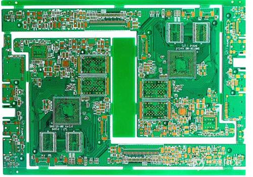
Schematic diagram, as the name implies, is a diagram showing the principle of connection between components on a circuit
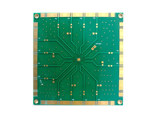
1. SMT patch processing link: Ten paste stir tin paste printing SPI stickers return welding aoi repairs. 2. DIP pl
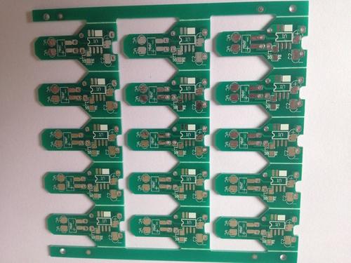
An important way to reduce EMI is to design the PCB ground plane. The first step is to make the ground area as large as p
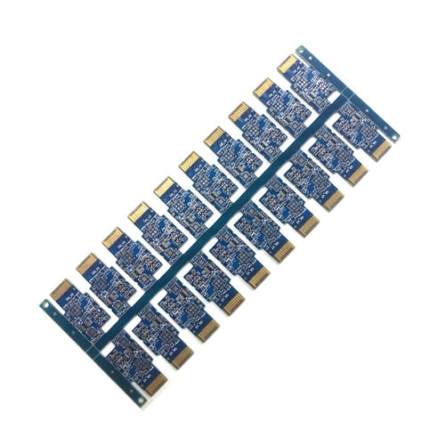
Presumably, the PCB circuit board laminate problem has puzzled everyone for a long time. After discussing with the engineer
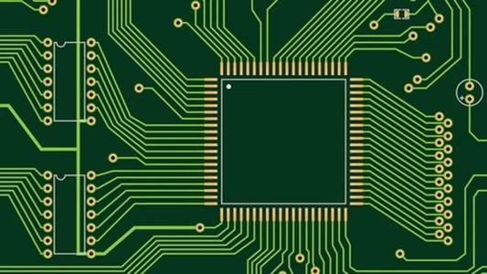
High-precision circuit board refers to the use of fine line width/spacing, tiny holes, narrow ring width (or no ring widt
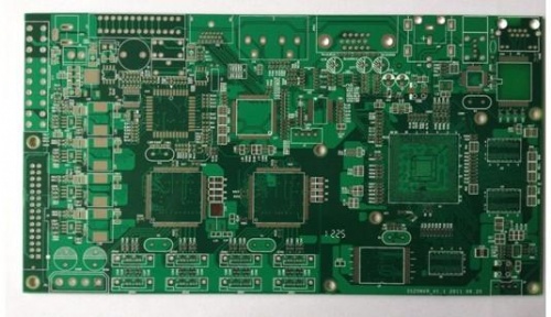
Looking at a complex PCB board, such as a computer's motherboard, you may find that several tracks have nowhere to go