

source:Industry News release time:2022-06-23 Article author:yu Popular:pcb
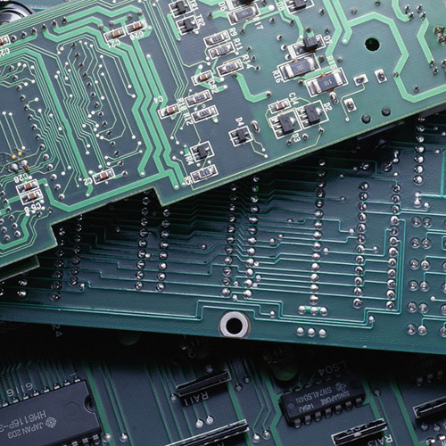
Speaking of blind and buried via boards, everyone's understanding and understanding of blind and buried via boards are very vague. Some circuit board manufacturers can't tell what is a blind and buried via board, how to look at it, and how it is. Blind hole board, what is a buried hole board, the definition and difference of a buried hole board; let's talk about the history of circuit boards: the name circuit board came from the 20th century before the beginning of the 21st century. Products have developed by leaps and bounds in technology, and electronic assembly technology has been rapidly improved. As a high-quality circuit board manufacturer of printed circuit boards, only continuous innovation and continuous improvement of the application range and performance of products can meet the needs of customers who are growing rapidly.
With the small, light and thin volume of electronic products in circuit board factories, printed circuit boards have developed flexible boards, rigid-flex boards, buried blind via boards, etc. First of all, let's start with traditional multi-layer boards. The structure of a standard multi-layer circuit board includes inner and outer layers, and then uses drilling and metallization processes in the holes to achieve the internal connection function of each layer of circuits. However, due to the increase in circuit density, the packaging method of parts is constantly updated. In order to allow more and higher performance parts to be placed in the limited circuit board area, in addition to the thinner circuit width, the aperture is also reduced from 1mm of DIP jack to 0.6mm of SMD, and further reduced to less than 0.4mm. However, it will still occupy the surface area, so there will be buried holes and blind holes. The definitions of buried holes and blind holes are as follows.
Buried Via
The buried hole is the through hole between the inner layers. After pressing, it cannot be seen, so it does not need to occupy the area of the outer layer. The upper and lower sides of the hole are in the inner layer of the circuit board, in other words, it is buried inside the circuit board. . To put it simply, it is sandwiched in the middle, and these processes cannot be seen from the surface. Therefore, before producing the buried hole board, you must carefully ask and understand the documents, or it will be troublesome!
Blind Via (BlindVia)
The blind hole plate is used for the connection between the surface layer and one or more inner layers. One side of the hole is on one side of the circuit board, and then it leads to the inside of the circuit board; simply put, the surface of the blind hole can see one side. The other side is in the circuit board, which is invisible, just like a well in our daily life. There is only one opening on the surface, and the water leads to the ground. For circuit board proofing, I recommend you to try it at the circuit board factory. Here, the circuit board proofing is priced online, with fast response, affordable price, fast speed and good quality. Through the above introduction, I hope everyone can have a certain understanding of the blind and buried hole board. learn.
Read recommendations:
Six-layer Immersion Gold Board (BGA)
Six-layer Immersion Gold Board (BGA)
Immersion gold process characteristics of PCB surface treatment!Automotive lighting PCB price
Popular recommended products
High frequency PCB
2021-04-27Six-layer Immersion Gold Board (BGA)
2021-04-27Six-layer Immersion Gold Board (BGA)
2021-05-27Six-layer Immersion Gold Board (BGA)
2021-05-24Single-sided double-layer AL base PCB
2021-04-27High frequency PCB
2021-04-27Six-layer Immersion Gold Board (BGA)
2021-04-27Silver oil perforated plate (double-sided)
2021-04-27Six-layer Immersion Gold Board (BGA)
2021-04-27Laminate copper-based PCB after 4L (sample)
2021-04-27Six-layer Immersion Gold Board (BGA)
2021-04-27Network communication board (sixth floor)
2021-04-29Computer card board (four layers)
2021-04-25Aluminum substrate (double-sided)
2021-04-27Display board (six layers)
2021-04-27Six-layer Immersion Gold Board (BGA)
2021-05-27Single copper base PCB
2021-04-27Six-layer Immersion Gold Board (BGA)
2021-05-24High frequency PCB
2021-04-27Mobile phone template (six layers)
2021-04-27Six-layer Immersion Gold Board (BGA)
2021-05-27High frequency PCB
2021-04-27Six-layer Immersion Gold Board (BGA)
2021-05-27SMT stickers
2021-05-27Six-layer Immersion Gold Board (BGA)
2021-04-26DIP plugin
2021-05-27DIP plugin
2021-05-27Mobile phone board
2021-04-27Six-layer Immersion Gold Board (BGA)
2021-04-26Six-layer Immersion Gold Board (BGA)
2021-04-26Six-layer Immersion Gold Board (BGA)
2021-04-26Six-layer Immersion Gold Board (BGA)
2021-04-26SMT stickers
2021-05-27Mobile phone board
2021-05-27Related Information
The relationship between PCB safety distance and voltage
2024-04-22SMT surface mount processing.Hybrid circuit board PCB
2024-04-15PCB enterprises should pay attention to SMT matters.Electronic components PCB
2024-04-03PCB - the core building block of electronic products.Automotive Electronics PCB
2024-03-25PCB - the bridge and link of the electronic world
2024-03-18How to define high-frequency and high-precision circuit boards.Industrial Electronics PCB
2024-03-11USB PCB interface layout and wiring requirements
2024-01-22Electrolytic capacitor PCB.Steps for using PCB pins
2024-01-15Automotive ElectronicWhat aspects should be considered when processing and manufacturing PCB boards?
2024-01-08Electrolytic capaciWhat is the difference between a gold-plated circuit board and a gold-plated one?
2023-12-25When grinding PCB boards, attention should be paid to.Oscillator (belonging to crystal) PCB
2023-12-18Industrial Electronics PCB!What precautions should be taken when copying and grinding PCB boards
2023-12-11Do you know who is more suitable for LED direct display, regarding the difference between PCB board
2023-12-05Aluminum electrolytic capacitor PCB.What are the standards for selecting PCB boards
2023-11-27Surface Mount Technology (SMT) Phase PCB
2023-11-20Oscillator (belonging to crystal) PCB.The main functions of PCB board
2023-11-13What is the difference between RO filter and PCB filter
2023-11-06Method for determining blind hole PCB board
2023-11-01Electronic Manufacturing Services PCB!What are the effects of PCB board color on performance?
2023-10-23Introduction to the Manufacturing Steps and Requirements of PCBA Test Stand
2023-10-16PCB version maturity stage.AOI circuit board price
2023-09-25How to maintain a PCB circuit board
2023-09-19Development Trend of Printed Circuit Board.Zener diode PCB Vendor
2023-09-14Common problems and cause analysis of PCB circuit board sampling.Zener diode PCB price
2023-09-08What are the issues that need to be understood in PCB circuit board design?IGBT module PCB factory
2023-09-08How to reduce the risk of bending and deformation in PCB circuit board production?Inverter PCB Produ
2023-08-16What are the three main factors that constitute welding defects in PCB circuit boards?Multilayer PCB
2023-08-16The structure of a glass teapot.LCD Module PCB factory
2023-08-11Glass teapot.Inverter PCB Processing
2023-08-11PCB online debugging
2023-08-08
CopyRight © 2007-2024Shenzhen Weienchen Technology Co., Ltd.
粤ICP备2021061255号

Address:
1205, Floor 12, Building 3, Chuangyi Office Building, No. 110, Ziheng West Road, Jinsha Community, Kengzi Street, Pingshan District, Shenzhen, Guangdong, China

Tel:
+86-755-29662580

Email:
sales@victoriapcb.com

PCB

PCBA
Service
Process
 Tel: +86-755-29662580
 Email: sales@victoriapcb.com
 中
中 current position:


