source:Industry News release time:2022-07-12 Article author:yu Popular:pcb

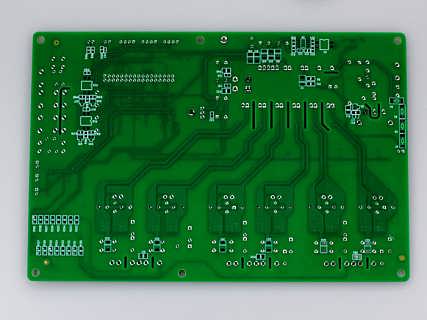
After the circuit board is patched, many users will encounter the situation that the vias are blocked. In those cases, the vias will be blocked. According to personal past experience, I will share the reasons why the vias are blocked after the patch. Of course, this reason is due to the production of circuit board manufacturers on the one hand, and the reason of SMT on the other hand. Analyze both aspects.
1. Defects caused by the drilling of the circuit board
The board produced by the circuit board is made of epoxy resin glass fiber. Referred to as FR4 fiberglass board. After the circuit board is drilled, there will be a layer of dust in the hole. Especially drill holes above 0.3MM. If the dust is not cleaned, copper cannot be deposited in the dusty place after curing, which will cause the via hole to be blocked. The defects caused by drilling can be tested if the PCB has been tested. This kind of bad circuit board manufacturers can do scrap processing.
2. Defects caused by copper sinking
The first choice is that the time for sinking copper is too short. The hole copper is not full. When the tin is applied, the hole copper melts off and causes defects. Most of these appear in vias below 0.3MM. The second is that the circuit board needs too much current without thickening the copper. After the power is turned on, the current is too large to melt the copper in the hole, which will cause defects. Therefore, if there is a PCB board that requires excessive current, it must be told to the circuit board manufacturer to thicken the copper during production. For example, circuit boards such as power supply boards are almost always made of thick copper plates.
3. Defects caused by SMT tin or flux quality and technology
This type of situation mostly occurs in the vias of the plug-in. The tin used by SMT manufacturers is not pure, and there are too many impurities. And the quality of the flux is too poor. Tin and tin welding is not good. This is easy to cause virtual welding. Components do not work. In addition, there are technical problems in SMT, which makes the circuit board stop flowing for too long when it passes through the tin furnace during soldering. Cause the hole copper to melt. The resulting vias are blocked
Read recommendations:
Six-layer Immersion Gold Board (BGA)
Six-layer Immersion Gold Board (BGA)
Quality control of PCB circuit board processing stage.Industrial Electronics PCB Wholesale
Popular recommended products
High frequency PCB
2021-04-27High frequency PCB
2021-04-27Six-layer Immersion Gold Board (BGA)
2021-05-27High frequency PCB
2021-04-27Laminate copper-based PCB after 4L (sample)
2021-04-27Six-layer Immersion Gold Board (BGA)
2021-04-27Six-layer Immersion Gold Board (BGA)
2021-05-24Computer card board (four layers)
2021-04-25Single copper base PCB
2021-04-27Six-layer Immersion Gold Board (BGA)
2021-05-27Silver oil perforated plate (double-sided)
2021-04-27Six-layer Immersion Gold Board (BGA)
2021-04-27Aluminum substrate (double-sided)
2021-04-27Network communication board (sixth floor)
2021-04-29Six-layer Immersion Gold Board (BGA)
2021-04-27Display board (six layers)
2021-04-27Mobile phone template (six layers)
2021-04-27Six-layer Immersion Gold Board (BGA)
2021-05-27Six-layer Immersion Gold Board (BGA)
2021-04-27Single-sided double-layer AL base PCB
2021-04-27High frequency PCB
2021-04-27Six-layer Immersion Gold Board (BGA)
2021-05-27Six-layer Immersion Gold Board (BGA)
2021-05-24SMT stickers
2021-05-27Mobile phone board
2021-04-27Six-layer Immersion Gold Board (BGA)
2021-04-26SMT stickers
2021-05-27DIP plugin
2021-05-27Mobile phone board
2021-05-27Six-layer Immersion Gold Board (BGA)
2021-04-26DIP plugin
2021-05-27Six-layer Immersion Gold Board (BGA)
2021-04-26Six-layer Immersion Gold Board (BGA)
2021-04-26Six-layer Immersion Gold Board (BGA)
2021-04-26Related Information
The relationship between PCB safety distance and voltage
2024-04-22SMT surface mount processing.Hybrid circuit board PCB
2024-04-15PCB enterprises should pay attention to SMT matters.Electronic components PCB
2024-04-03PCB - the core building block of electronic products.Automotive Electronics PCB
2024-03-25PCB - the bridge and link of the electronic world
2024-03-18How to define high-frequency and high-precision circuit boards.Industrial Electronics PCB
2024-03-11USB PCB interface layout and wiring requirements
2024-01-22Electrolytic capacitor PCB.Steps for using PCB pins
2024-01-15Automotive ElectronicWhat aspects should be considered when processing and manufacturing PCB boards?
2024-01-08Electrolytic capaciWhat is the difference between a gold-plated circuit board and a gold-plated one?
2023-12-25When grinding PCB boards, attention should be paid to.Oscillator (belonging to crystal) PCB
2023-12-18Industrial Electronics PCB!What precautions should be taken when copying and grinding PCB boards
2023-12-11Do you know who is more suitable for LED direct display, regarding the difference between PCB board
2023-12-05Aluminum electrolytic capacitor PCB.What are the standards for selecting PCB boards
2023-11-27Surface Mount Technology (SMT) Phase PCB
2023-11-20Oscillator (belonging to crystal) PCB.The main functions of PCB board
2023-11-13What is the difference between RO filter and PCB filter
2023-11-06Method for determining blind hole PCB board
2023-11-01Electronic Manufacturing Services PCB!What are the effects of PCB board color on performance?
2023-10-23Introduction to the Manufacturing Steps and Requirements of PCBA Test Stand
2023-10-16PCB version maturity stage.AOI circuit board price
2023-09-25How to maintain a PCB circuit board
2023-09-19Development Trend of Printed Circuit Board.Zener diode PCB Vendor
2023-09-14Common problems and cause analysis of PCB circuit board sampling.Zener diode PCB price
2023-09-08What are the issues that need to be understood in PCB circuit board design?IGBT module PCB factory
2023-09-08How to reduce the risk of bending and deformation in PCB circuit board production?Inverter PCB Produ
2023-08-16What are the three main factors that constitute welding defects in PCB circuit boards?Multilayer PCB
2023-08-16The structure of a glass teapot.LCD Module PCB factory
2023-08-11Glass teapot.Inverter PCB Processing
2023-08-11PCB online debugging
2023-08-08