

source:Industry News release time:2022-06-20 Article author:yu Popular:pcb
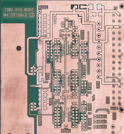
Critical components require pre-checkpoints on the PCB. The pads used for soldering surface mount components are not allowed to double as inspection points, and other preset dedicated inspection pads are necessary to ensure that solder joint inspection and production debugging can be carried out without problems. The pads used for inspection are arranged on one side of the PCB as much as possible, even for inspection, which is beneficial to reduce the cost of inspection.
1. Process preset requirements
(1) The distance between the inspection point and the edge of the PCB should be greater than 5mm;
(2) The inspection point cannot be covered by solder mask or text ink;
(3) The size, distance and layout of the inspection point pads should also match the relevant requirements of the inspection equipment used;
(4) The inspection point should be placed 1mm away from the element to prevent the probe and element from colliding;
(5) The best solder plating at the inspection point or the use of softer, easy-to-penetrate, and non-oxidative metals to ensure that they are grounded and extend the service life of the probe;
(6) The diameter of the inspection point is not less than 0.4mm, and the distance between adjacent inspection points is more than 2.54mm, but not less than 1.27mm;
(7) Components with a height of more than 6.4mm cannot be placed on the inspection surface. Too high components will cause poor contact between the probes of the online inspection fixture and the inspection points;
⑻ The distance C from the center of the inspection point to the end edge of the chip component is related to the SMD height H as follows: SMD height H≤3mm, C≥2mm; SMD height H≥3mm, C≥4mm.
(9) The inspection point should be placed in the positioning hole (cooperative inspection point is used for precise positioning, preferably non-metallized hole, the error of the positioning hole should be within ±0.05mm) 3.2mm around the ring;
2. Electrical Preset Requirements
(1) The inspection points should be evenly distributed on the PCB circuit board to reduce the compressive stress of the probe;
(2) When setting the check point on the circuit trace, its width can be expanded to 1mm;
(3) Each electrical contact needs to have a check point, and each IC needs to have a power and ground check point, and it should be as close as possible to the components, and most fortunately, within 2.54mm;
(4) Try to lead the SMC/SMD inspection point on the component surface to the welding surface through the via hole, the diameter of the via hole is greater than 1mm, and the single-sided needle bed can be used for inspection to reduce the inspection cost;
(5) The power supply line on the PCB circuit board should be set up with check breakpoints in different regions, so that the power supply can be decoupled or blocked. When setting breakpoints, consideration should be given to the power-carrying capacity after the breakpoint is recovered and checked.
Read recommendations:
Six-layer Immersion Gold Board (BGA)
Mobile phone template (six layers)
Popular recommended products
High frequency PCB
2021-04-27Six-layer Immersion Gold Board (BGA)
2021-05-24Six-layer Immersion Gold Board (BGA)
2021-04-27Laminate copper-based PCB after 4L (sample)
2021-04-27High frequency PCB
2021-04-27Six-layer Immersion Gold Board (BGA)
2021-05-24Six-layer Immersion Gold Board (BGA)
2021-05-27High frequency PCB
2021-04-27Network communication board (sixth floor)
2021-04-29Six-layer Immersion Gold Board (BGA)
2021-05-27Mobile phone template (six layers)
2021-04-27Aluminum substrate (double-sided)
2021-04-27High frequency PCB
2021-04-27Six-layer Immersion Gold Board (BGA)
2021-05-27Six-layer Immersion Gold Board (BGA)
2021-04-27Six-layer Immersion Gold Board (BGA)
2021-04-27Six-layer Immersion Gold Board (BGA)
2021-05-27Silver oil perforated plate (double-sided)
2021-04-27Computer card board (four layers)
2021-04-25Display board (six layers)
2021-04-27Single copper base PCB
2021-04-27Six-layer Immersion Gold Board (BGA)
2021-04-27Single-sided double-layer AL base PCB
2021-04-27Mobile phone board
2021-05-27Six-layer Immersion Gold Board (BGA)
2021-04-26Mobile phone board
2021-04-27Six-layer Immersion Gold Board (BGA)
2021-04-26Six-layer Immersion Gold Board (BGA)
2021-04-26SMT stickers
2021-05-27DIP plugin
2021-05-27Six-layer Immersion Gold Board (BGA)
2021-04-26Six-layer Immersion Gold Board (BGA)
2021-04-26SMT stickers
2021-05-27DIP plugin
2021-05-27Related Information
The relationship between PCB safety distance and voltage
2024-04-22SMT surface mount processing.Hybrid circuit board PCB
2024-04-15PCB enterprises should pay attention to SMT matters.Electronic components PCB
2024-04-03PCB - the core building block of electronic products.Automotive Electronics PCB
2024-03-25PCB - the bridge and link of the electronic world
2024-03-18How to define high-frequency and high-precision circuit boards.Industrial Electronics PCB
2024-03-11USB PCB interface layout and wiring requirements
2024-01-22Electrolytic capacitor PCB.Steps for using PCB pins
2024-01-15Automotive ElectronicWhat aspects should be considered when processing and manufacturing PCB boards?
2024-01-08Electrolytic capaciWhat is the difference between a gold-plated circuit board and a gold-plated one?
2023-12-25When grinding PCB boards, attention should be paid to.Oscillator (belonging to crystal) PCB
2023-12-18Industrial Electronics PCB!What precautions should be taken when copying and grinding PCB boards
2023-12-11Do you know who is more suitable for LED direct display, regarding the difference between PCB board
2023-12-05Aluminum electrolytic capacitor PCB.What are the standards for selecting PCB boards
2023-11-27Surface Mount Technology (SMT) Phase PCB
2023-11-20Oscillator (belonging to crystal) PCB.The main functions of PCB board
2023-11-13What is the difference between RO filter and PCB filter
2023-11-06Method for determining blind hole PCB board
2023-11-01Electronic Manufacturing Services PCB!What are the effects of PCB board color on performance?
2023-10-23Introduction to the Manufacturing Steps and Requirements of PCBA Test Stand
2023-10-16PCB version maturity stage.AOI circuit board price
2023-09-25How to maintain a PCB circuit board
2023-09-19Development Trend of Printed Circuit Board.Zener diode PCB Vendor
2023-09-14Common problems and cause analysis of PCB circuit board sampling.Zener diode PCB price
2023-09-08What are the issues that need to be understood in PCB circuit board design?IGBT module PCB factory
2023-09-08How to reduce the risk of bending and deformation in PCB circuit board production?Inverter PCB Produ
2023-08-16What are the three main factors that constitute welding defects in PCB circuit boards?Multilayer PCB
2023-08-16The structure of a glass teapot.LCD Module PCB factory
2023-08-11Glass teapot.Inverter PCB Processing
2023-08-11PCB online debugging
2023-08-08
CopyRight © 2007-2024Shenzhen Weienchen Technology Co., Ltd.
粤ICP备2021061255号

Address:
1205, Floor 12, Building 3, Chuangyi Office Building, No. 110, Ziheng West Road, Jinsha Community, Kengzi Street, Pingshan District, Shenzhen, Guangdong, China

Tel:
+86-755-29662580

Email:
sales@victoriapcb.com

PCB

PCBA
Service
Process
 Tel: +86-755-29662580
 Email: sales@victoriapcb.com
 中
中 current position:


