
source:Optimization dedicated release time:2022-04-15 Article author:yu Popular:pcb
I. Introduction
The purpose of etching: After the circuit is electroplated, the PCB circuit board removed from the electroplating equipment is processed to complete the circuit board. Specifically, there are the following steps:
a. Peel off the film: peel off the dry film for anti-plating purposes with the potion. The hardened dry film is partially dissolved under the dope, and partially peeled off into flakes. In order to maintain the effect of the liquid and the completeness of the post-washing, the efficiency of the filtration system is very important.
b. Line etching: dissolve the copper in the non-conductor part.
c. Stripping tin and lead: Finally, remove the anti-etching tin-lead coating. Regardless of pure tin or the tin-lead layer of each composition ratio, the purpose of plating is only for anti-etching, so after the etching is completed, it must be stripped off, so this step of stripping tin-lead is only for processing, and no added value is generated. But the following points still need special attention, otherwise the cost increase is the second, and the outer layer circuit that is finally completed will cause defects here.
At present, the typical process of printed circuit board (PCB) processing adopts "pattern plating method". That is, pre-plating a lead-tin resist layer on the copper foil part that needs to be retained on the outer layer of the board, that is, the graphic part of the circuit, and then chemically corrode the rest of the copper foil.
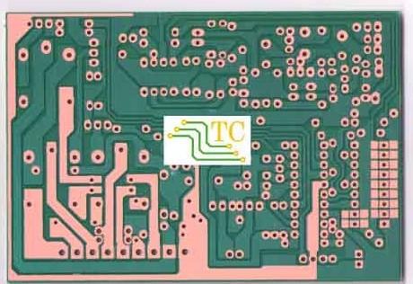
PCB multilayer circuit board/circuit board
PCB multilayer circuit board/circuit board
It should be noted that there are two layers of copper on the PCB board at this time. In the outer layer etching process, only one layer of copper must be completely etched away, and the rest will form the final required circuit. This type of pattern plating is characterized by the presence of a copper layer only under the lead-tin resist. Another process method is to coat the entire board with copper, and the part other than the photosensitive film is only a tin or lead-tin resist layer. This process is called "full board copper plating process". Compared with pattern plating, the biggest disadvantage of full-board copper plating is that copper is plated twice everywhere on the board and must be etched away during etching. Therefore, a series of problems will arise when the wire width is very fine. At the same time, side corrosion can seriously affect the uniformity of the lines.
In the processing technology of the outer circuit of the PCB printed circuit board, there is another method, which is to use the photosensitive film instead of the metal coating as the resist layer. This method is very similar to the inner layer etching process, you can refer to the etching in the inner layer fabrication process.
At present, tin or lead tin is the most commonly used resist layer, which is used in the etching process of ammonia etchant. Ammonia etchant is a commonly used chemical liquid, which does not have any chemical reaction with tin or lead tin. Ammonia etchant mainly refers to ammonia water/ammonium chloride etching solution. In addition, ammonia water/ammonia sulfate etching solution is also available in the market.
Sulfate-based etching solution, after use, the copper in it can be separated by electrolysis, so it can be reused. Due to its low corrosion rate, it is generally rare in actual production, but it is expected to be used in chlorine-free etching. Some people tried to use sulfuric acid-hydrogen peroxide as an etchant to corrode the outer layer pattern. For many reasons including economics and waste disposal aspects, this process has not yet been adopted in a commercial sense. Furthermore, sulfuric acid-hydrogen peroxide cannot be used for the etching of lead-tin resist, and this process is not the main method in the production of the outer layer of PCB, so most people rarely care about it.
2. Equipment adjustment and interaction with corrosive solution
In the processing of printed circuit boards, ammonia etching is a relatively fine and complex chemical reaction process. In turn it is an easy job. Once the process has been turned up, production can continue. The key is that once it is turned on, it needs to maintain a continuous working state, and it is not advisable to stop and stop. The etching process depends to a great extent on the good working condition of the equipment. At present, no matter what kind of etching solution is used, high-pressure spraying must be used, and in order to obtain neat line sides and high-quality etching effect, the structure and spraying method of the nozzle must be strictly selected.
In order to obtain a good side effect, many different theories have emerged, resulting in different design methods and equipment structures. These theories are often very different. But all theories about etching acknowledge the basic principle of getting the metal surface in constant contact with fresh etchant as quickly as possible. The chemical mechanism analysis of the etching process also confirmed the above point. In ammonia etching, assuming all other parameters are constant, the etching rate is mainly determined by the ammonia (NH3) in the etching solution. Therefore, using a fresh solution to interact with the etching surface has two main purposes: one is to flush out the copper ions just produced; the other is to continuously provide the ammonia (NH3) required for the reaction.
In the traditional knowledge of the printed circuit board (PCB) industry, especially the suppliers of printed circuit raw materials, it is generally recognized that the lower the content of monovalent copper ions in the ammonia-based etching solution, the faster the reaction speed. This has been confirmed by experience. In fact, many ammonia-based etchant products contain special ligands (some complex solvents) for monovalent copper ions, which act to reduce monovalent copper ions (these are the technical secrets of their products' high reactivity ), it can be seen that the influence of monovalent copper ions is not small. Reducing the monovalent copper from 5000ppm to 50ppm will more than double the etch rate.
Since a large amount of monovalent cupric ions are generated during the etching reaction, and because monovalent cupric ions are always tightly combined with the complex group of ammonia, it is very difficult to keep the content close to zero. Monovalent copper can be removed by converting monovalent copper to divalent copper by the action of oxygen in the atmosphere. The above purpose can be achieved by spraying.
This is one functional reason to pass air into the etching chamber. However, if there is too much air, it will accelerate the loss of ammonia in the solution and reduce the pH value, which will still reduce the etch rate. Ammonia is also a variable amount in solution that needs to be controlled. Some users have adopted the practice of passing pure ammonia into the etching reservoir. To do so, a PH meter control system must be added. When the automatically measured pH is lower than a given value, the solution is automatically added.
In the related field of chemical etching (also known as photochemical etching or PCH), research work has begun and has reached the stage of structural design of the etcher. In this method, the solution used is copper divalent, not an ammonia-copper etch. It will likely be used in the printed circuit industry. In the PCH industry, the typical thickness of etched copper foil is 5 to 10 mils (mils), and in some cases the thickness is quite large. Its requirements for etching parameters are often more stringent than those in the PCB industry.
There is a study from PCM industrial systems that has not yet been officially published, but the results will be refreshing. Because of the relatively strong project funding support, the researchers have the ability to change the design thinking of the etching device in the long term and study the effects of these changes. For example, compared to conical nozzles, the optimal nozzle design is fan-shaped, and the spray manifold (that is, the tube into which the nozzle is screwed) also has an installation angle that can spray the workpiece entering the etching chamber at a 30 degree angle. Without such a change, the nozzles on the manifold are mounted in such a way that the spray angle of each adjacent nozzle is not exactly the same. The respective spray surfaces of the second group of nozzles are slightly different from those of the first group (it represents the operation of the spray). In this way, the shapes of the sprayed solutions are superimposed or crossed. Theoretically, if the solution shapes cross each other, the jetting force of that part is reduced and cannot effectively wash the old solution off the etched surface while keeping the new solution in contact with it. This is especially true at the edges of the spray surface. Its jet force is much smaller than that in the vertical direction.
This study found that the latest design parameter is 65 psi (ie 4+Bar). Every etching process and every practical solution has an optimum injection pressure, and at present, it is very rare that the injection pressure in the etching chamber exceeds 30 psi (2Bar). There is a principle that the higher the density of an etching solution (ie specific gravity or degree of Bomer), the higher the optimum injection pressure should be. Of course this is not a single parameter. Another important parameter is the relative mobility (or mobility) that controls its reaction rate in solution.
3. Etching quality and early problems
The basic requirement for etching quality is to be able to completely remove all copper layers except under the resist layer, and that's it. Strictly speaking, if it is to be accurately defined, the etching quality must include the consistency of the wire width and the degree of undercut. Due to the inherent characteristics of the current etchant, it not only etches downward but also in all directions, so side etching is almost inevitable.
The problem of undercut is one of the etching parameters that is often discussed. It is defined as the ratio of the width of the undercut to the depth of the etching, which is called the etching factor. In the printed circuit industry, it varies widely, from 1:1 to 1:5. Obviously, a small undercut degree or a low etch factor is the most satisfactory.
The structure of the etching equipment and the different compositions of the etching solution will have an impact on the etching factor or side etching degree, or in optimistic terms, it can be controlled. The use of certain additives can reduce the degree of side etching. The chemical compositions of these additives are generally trade secrets, and their developers do not disclose them to the outside world.
In many ways, the quality of etching exists long before the printed board enters the etching machine. Because there is a very close internal connection between the various processes or processes of printed circuit processing, there is no process that is not affected by other processes and does not affect other processes. Many of the problems identified as etch quality actually existed in the stripping process even earlier. For the etching process of the outer layer pattern, because the "reverse stream" phenomenon it reflects is more prominent than most printed board processes, many problems are finally reflected on it. At the same time, this is also because the etching is the last link in a long series of processes starting with self-adhesive film and photosensitive. After that, the outer layer pattern is successfully transferred. The more links there are, the greater the chance of problems. This can be seen as a very special aspect of the printed circuit production process.
Theoretically, after the printed circuit enters the etching stage, in the process of processing the printed circuit by the pattern plating method, the ideal state should be: the sum of the thicknesses of copper and tin or copper and lead-tin after electroplating should not exceed the electroplating resistance The thickness of the photosensitive film, so that the electroplating pattern is completely blocked by the "walls" on both sides of the film and embedded in it. However, in actual production, after electroplating of printed circuit boards all over the world, the coating pattern is much thicker than the photosensitive pattern. In the process of electroplating copper and lead-tin, since the height of the plating layer exceeds the photosensitive film, there is a tendency to accumulate laterally, and the problem arises. The tin or lead-tin resist covered above the lines extends to both sides to form "edges", and a small part of the photosensitive film is covered under the "edges".
The "edge" formed by tin or lead-tin makes it impossible to completely remove the photosensitive film when removing the film, leaving a small part of "residual glue" under the "edge". "Residual glue" or "residual film" is left under the resist "edge" and will cause incomplete etching. The lines form "copper roots" on both sides after etching, and the copper roots narrow the line spacing, resulting in the printed board not meeting the requirements of Party A, and may even be rejected. The production cost of the PCB circuit board will be greatly increased due to rejection.
In addition, in many cases, due to the formation of dissolution due to the reaction, in the printed circuit industry, the residual film and copper may also form deposits in the etching solution and block the nozzle of the etching machine and the acid-resistant pump, and have to be shut down for processing and cleaning. , which affects work efficiency.
Fourth, the maintenance of etching equipment
The most critical factor in the maintenance of etching equipment is to ensure that the nozzles are clean and free of obstructions to make the spraying smooth. Blockages or slagging can impact the layout under the jet pressure. If the nozzle is not clean, the etching will be uneven and the entire PCB will be scrapped.
Obviously, the maintenance of the equipment is to replace the damaged and worn parts, including the replacement of the nozzle, which also has the problem of wear and tear. In addition, the more critical issue is to keep the etching machine free of slagging, and slag accumulation will occur in many cases. Too much slag accumulation will even affect the chemical balance of the etching solution. Likewise, if the etchant exhibits an excessive chemical imbalance, slag formation will be exacerbated. The problem of slag buildup cannot be overemphasized. Once a large amount of slagging occurs suddenly in the etching solution, it is usually a signal that there is a problem with the balance of the solution. This should be properly cleaned with stronger hydrochloric acid or the solution should be replenished.
Residual film can also produce slag, a very small amount of residual film is dissolved in the etching solution, and then the copper salt precipitate is formed. The slag formed by the residual film indicates that the previous film removal process is not complete. Poor film removal is often the result of a combination of edge film and overplating.
Read recommendations:
Aluminum substrate (double-sided)
Computer card board (four layers)
Major reform of PCB manufacturers!Aluminum electrolytic capacitor PCB
Popular recommended products
Computer card board (four layers)
2021-04-25Single copper base PCB
2021-04-27Silver oil perforated plate (double-sided)
2021-04-27High frequency PCB
2021-04-27Six-layer Immersion Gold Board (BGA)
2021-05-27High frequency PCB
2021-04-27Six-layer Immersion Gold Board (BGA)
2021-05-24High frequency PCB
2021-04-27Laminate copper-based PCB after 4L (sample)
2021-04-27Aluminum substrate (double-sided)
2021-04-27Six-layer Immersion Gold Board (BGA)
2021-05-24Six-layer Immersion Gold Board (BGA)
2021-04-27Single-sided double-layer AL base PCB
2021-04-27Six-layer Immersion Gold Board (BGA)
2021-05-27Six-layer Immersion Gold Board (BGA)
2021-04-27Six-layer Immersion Gold Board (BGA)
2021-05-27Six-layer Immersion Gold Board (BGA)
2021-04-27High frequency PCB
2021-04-27Display board (six layers)
2021-04-27Network communication board (sixth floor)
2021-04-29Six-layer Immersion Gold Board (BGA)
2021-04-27Mobile phone template (six layers)
2021-04-27Six-layer Immersion Gold Board (BGA)
2021-05-27Six-layer Immersion Gold Board (BGA)
2021-04-26SMT stickers
2021-05-27DIP plugin
2021-05-27Six-layer Immersion Gold Board (BGA)
2021-04-26Mobile phone board
2021-05-27Mobile phone board
2021-04-27Six-layer Immersion Gold Board (BGA)
2021-04-26Six-layer Immersion Gold Board (BGA)
2021-04-26SMT stickers
2021-05-27DIP plugin
2021-05-27Six-layer Immersion Gold Board (BGA)
2021-04-26Related Information
The relationship between PCB safety distance and voltage
2024-04-22SMT surface mount processing.Hybrid circuit board PCB
2024-04-15PCB enterprises should pay attention to SMT matters.Electronic components PCB
2024-04-03PCB - the core building block of electronic products.Automotive Electronics PCB
2024-03-25PCB - the bridge and link of the electronic world
2024-03-18How to define high-frequency and high-precision circuit boards.Industrial Electronics PCB
2024-03-11USB PCB interface layout and wiring requirements
2024-01-22Electrolytic capacitor PCB.Steps for using PCB pins
2024-01-15Automotive ElectronicWhat aspects should be considered when processing and manufacturing PCB boards?
2024-01-08Electrolytic capaciWhat is the difference between a gold-plated circuit board and a gold-plated one?
2023-12-25When grinding PCB boards, attention should be paid to.Oscillator (belonging to crystal) PCB
2023-12-18Industrial Electronics PCB!What precautions should be taken when copying and grinding PCB boards
2023-12-11Do you know who is more suitable for LED direct display, regarding the difference between PCB board
2023-12-05Aluminum electrolytic capacitor PCB.What are the standards for selecting PCB boards
2023-11-27Surface Mount Technology (SMT) Phase PCB
2023-11-20Oscillator (belonging to crystal) PCB.The main functions of PCB board
2023-11-13What is the difference between RO filter and PCB filter
2023-11-06Method for determining blind hole PCB board
2023-11-01Electronic Manufacturing Services PCB!What are the effects of PCB board color on performance?
2023-10-23Introduction to the Manufacturing Steps and Requirements of PCBA Test Stand
2023-10-16PCB version maturity stage.AOI circuit board price
2023-09-25How to maintain a PCB circuit board
2023-09-19Development Trend of Printed Circuit Board.Zener diode PCB Vendor
2023-09-14Common problems and cause analysis of PCB circuit board sampling.Zener diode PCB price
2023-09-08What are the issues that need to be understood in PCB circuit board design?IGBT module PCB factory
2023-09-08How to reduce the risk of bending and deformation in PCB circuit board production?Inverter PCB Produ
2023-08-16What are the three main factors that constitute welding defects in PCB circuit boards?Multilayer PCB
2023-08-16The structure of a glass teapot.LCD Module PCB factory
2023-08-11Glass teapot.Inverter PCB Processing
2023-08-11PCB online debugging
2023-08-08
CopyRight © 2007-2024Shenzhen Weienchen Technology Co., Ltd.
粤ICP备2021061255号

Address:
1205, Floor 12, Building 3, Chuangyi Office Building, No. 110, Ziheng West Road, Jinsha Community, Kengzi Street, Pingshan District, Shenzhen, Guangdong, China

Tel:
+86-755-29662580

Email:
sales@victoriapcb.com

PCB

PCBA
Service
Process
 Tel: +86-755-29662580
 Email: sales@victoriapcb.com
 中
中 current position:


