source:Industry News release time:2022-04-09 Article author:sznbone Popular:pcb
1. Spacing between wires
As far as the processing capabilities of mainstream Shenzhen PCB manufacturers are concerned, the minimum distance between wires should not be less than 4mil. The minimum line spacing is also the line-to-line and line-to-pad distance. From the production point of view, the bigger the better under conditions, the more common one is 10mil.
2. Pad aperture and pad width
As far as the processing capabilities of mainstream Shenzhen PCB manufacturers are concerned, if the pad diameter is mechanically drilled, the minimum should not be less than 0.2mm, and if the laser drilling method is used, the minimum should not be less than 4mil. The hole diameter tolerance is slightly different according to the different plates. Generally, it can be controlled within 0.05mm, and the minimum pad width should not be less than 0.2mm.
If it is a large area of copper, usually there is a shrinking distance from the edge of the board, which is generally set to 20mil. In the PCB design and manufacturing industry, under normal circumstances, for the sake of mechanical considerations of the finished circuit board, or to avoid the occurrence of curling or electrical short circuit due to the exposed copper skin on the edge of the board, engineers often place copper on a large area. Instead of laying copper all the way to the edge of the board, the block is indented by 20 mils relative to the edge of the board.
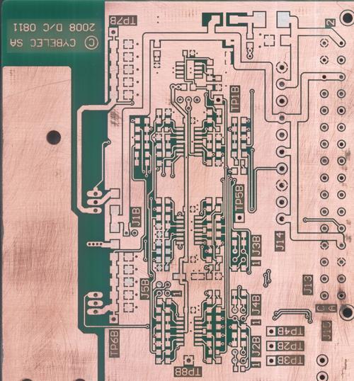
Double-sided pcb circuit board
There are many ways to deal with this copper skin shrinking, such as drawing the keepout layer on the edge of the board, and then setting the distance between the copper and the keepout. Here is a simple method, that is, to set different safety distances for the copper objects, for example, set the safety distance of the whole board to 10mil, and set the copper to 20mil, you can achieve the effect of shrinking the edge of the board by 20mil. Removed dead copper that may have occurred within the device.
Non-electrically related safety distances
No changes can be made to the text film during processing, but the width of the character lines whose D-CODE is less than 0.22mm (8.66mil) is thickened to 0.22mm, that is, the width of the character line is L=0.22mm (8.66mil).
The width of the whole character is W=1.0mm, the height of the whole character is H=1.2mm, and the spacing between characters is D=0.2mm. When the text is smaller than the above standard, the processing and printing will be blurred.
Via-to-via spacing
The silk screen is not allowed to cover the pads. Because if the silk screen is covered with the pad, the silk screen will not be able to be tinned when tinning, which will affect the mounting of components. Generally, the circuit board factory requires a spacing of 8 mils to be reserved. If the area of the circuit board is limited, the spacing of 4mil is barely acceptable. If the silk screen accidentally covers the pad during the design, the circuit board factory will automatically eliminate the silk screen part left on the pad during manufacture to ensure that the pad is tinned.
Read recommendations:
Network communication board (sixth floor)
Mobile phone template (six layers)
The difference between positive and negative PCB circuit board
Popular recommended products
Six-layer Immersion Gold Board (BGA)
2021-05-27Six-layer Immersion Gold Board (BGA)
2021-04-27High frequency PCB
2021-04-27Display board (six layers)
2021-04-27Mobile phone template (six layers)
2021-04-27Six-layer Immersion Gold Board (BGA)
2021-05-27Aluminum substrate (double-sided)
2021-04-27High frequency PCB
2021-04-27Six-layer Immersion Gold Board (BGA)
2021-05-24Network communication board (sixth floor)
2021-04-29Computer card board (four layers)
2021-04-25Single-sided double-layer AL base PCB
2021-04-27Silver oil perforated plate (double-sided)
2021-04-27Six-layer Immersion Gold Board (BGA)
2021-05-27High frequency PCB
2021-04-27Single copper base PCB
2021-04-27Six-layer Immersion Gold Board (BGA)
2021-05-27Six-layer Immersion Gold Board (BGA)
2021-04-27High frequency PCB
2021-04-27Six-layer Immersion Gold Board (BGA)
2021-05-24Six-layer Immersion Gold Board (BGA)
2021-04-27Six-layer Immersion Gold Board (BGA)
2021-04-27Laminate copper-based PCB after 4L (sample)
2021-04-27Six-layer Immersion Gold Board (BGA)
2021-04-26SMT stickers
2021-05-27Six-layer Immersion Gold Board (BGA)
2021-04-26Mobile phone board
2021-04-27Six-layer Immersion Gold Board (BGA)
2021-04-26Six-layer Immersion Gold Board (BGA)
2021-04-26DIP plugin
2021-05-27DIP plugin
2021-05-27Six-layer Immersion Gold Board (BGA)
2021-04-26Mobile phone board
2021-05-27SMT stickers
2021-05-27Related Information
The relationship between PCB safety distance and voltage
2024-04-22SMT surface mount processing.Hybrid circuit board PCB
2024-04-15PCB enterprises should pay attention to SMT matters.Electronic components PCB
2024-04-03PCB - the core building block of electronic products.Automotive Electronics PCB
2024-03-25PCB - the bridge and link of the electronic world
2024-03-18How to define high-frequency and high-precision circuit boards.Industrial Electronics PCB
2024-03-11USB PCB interface layout and wiring requirements
2024-01-22Electrolytic capacitor PCB.Steps for using PCB pins
2024-01-15Automotive ElectronicWhat aspects should be considered when processing and manufacturing PCB boards?
2024-01-08Electrolytic capaciWhat is the difference between a gold-plated circuit board and a gold-plated one?
2023-12-25When grinding PCB boards, attention should be paid to.Oscillator (belonging to crystal) PCB
2023-12-18Industrial Electronics PCB!What precautions should be taken when copying and grinding PCB boards
2023-12-11Do you know who is more suitable for LED direct display, regarding the difference between PCB board
2023-12-05Aluminum electrolytic capacitor PCB.What are the standards for selecting PCB boards
2023-11-27Surface Mount Technology (SMT) Phase PCB
2023-11-20Oscillator (belonging to crystal) PCB.The main functions of PCB board
2023-11-13What is the difference between RO filter and PCB filter
2023-11-06Method for determining blind hole PCB board
2023-11-01Electronic Manufacturing Services PCB!What are the effects of PCB board color on performance?
2023-10-23Introduction to the Manufacturing Steps and Requirements of PCBA Test Stand
2023-10-16PCB version maturity stage.AOI circuit board price
2023-09-25How to maintain a PCB circuit board
2023-09-19Development Trend of Printed Circuit Board.Zener diode PCB Vendor
2023-09-14Common problems and cause analysis of PCB circuit board sampling.Zener diode PCB price
2023-09-08What are the issues that need to be understood in PCB circuit board design?IGBT module PCB factory
2023-09-08How to reduce the risk of bending and deformation in PCB circuit board production?Inverter PCB Produ
2023-08-16What are the three main factors that constitute welding defects in PCB circuit boards?Multilayer PCB
2023-08-16The structure of a glass teapot.LCD Module PCB factory
2023-08-11Glass teapot.Inverter PCB Processing
2023-08-11PCB online debugging
2023-08-08