source:Industry News release time:2024-07-09 Article author:yu Popular:pcb

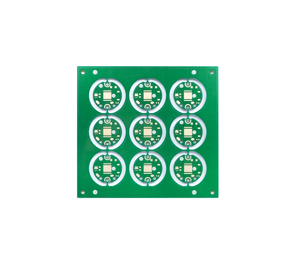
The process of making a PCB board (printed circuit board) usually includes the following main steps:
1. Design: Designers use CAD software to draw circuit design diagrams, determine the position and connection method of circuit components.
2. Plate making: Produce the designed circuit diagram into a film (similar to a transparent film template) for subsequent graphic transfer.
3. Drilling: According to the circuit design diagram, drill corresponding holes on the copper clad plate, which will be used for installing electronic components or as conductive holes to connect circuits of different layers.
4. Copper sinking: A thin layer of copper is deposited on the surface of the board after drilling, in order to form a conductive path in the non-conductive area.
5. Graphic transfer: Transfer the circuit pattern from the film to the copper-clad board, usually achieved using photosensitive resin and UV exposure.
6. Etching: By using chemical or electrochemical etching methods, the copper layer that has not been covered by pattern transfer is removed to form a circuit pattern.
7. Tin/Gold Plating: In order to protect the circuit board and enhance its soldering performance, a layer of tin or gold is usually plated on the surface of the circuit board.
8. Screen printing: Printing component identification and other necessary information on a circuit board for subsequent assembly and maintenance.
9. Assembly: Solder various electronic components onto the circuit board to form a complete electronic device.
10. Testing: Perform functional testing on the assembled circuit board to ensure its normal operation.
11. Packaging: Package the tested circuit boards and prepare them for delivery to customers or enter the next production process.
The above is a common PCB board manufacturing process, and the specific steps may vary depending on different manufacturing processes and requirements.
Read recommendations:
Mobile phone template (six layers)
Six-layer Immersion Gold Board (BGA)
Six-layer Immersion Gold Board (BGA)
Introduction to the problems of AOI detection in SMT chip processing.Industrial Electronics PCB Whol
Popular recommended products
Display board (six layers)
2021-04-27Six-layer Immersion Gold Board (BGA)
2021-04-27Six-layer Immersion Gold Board (BGA)
2021-05-27Six-layer Immersion Gold Board (BGA)
2021-05-27Six-layer Immersion Gold Board (BGA)
2021-04-27High frequency PCB
2021-04-27Six-layer Immersion Gold Board (BGA)
2021-04-27Laminate copper-based PCB after 4L (sample)
2021-04-27Six-layer Immersion Gold Board (BGA)
2021-05-24Single copper base PCB
2021-04-27Six-layer Immersion Gold Board (BGA)
2021-05-27Six-layer Immersion Gold Board (BGA)
2021-04-27Six-layer Immersion Gold Board (BGA)
2021-05-27Network communication board (sixth floor)
2021-04-29Aluminum substrate (double-sided)
2021-04-27High frequency PCB
2021-04-27High frequency PCB
2021-04-27Computer card board (four layers)
2021-04-25High frequency PCB
2021-04-27Silver oil perforated plate (double-sided)
2021-04-27Single-sided double-layer AL base PCB
2021-04-27Six-layer Immersion Gold Board (BGA)
2021-05-24Mobile phone template (six layers)
2021-04-27Six-layer Immersion Gold Board (BGA)
2021-04-26DIP plugin
2021-05-27Six-layer Immersion Gold Board (BGA)
2021-04-26Six-layer Immersion Gold Board (BGA)
2021-04-26Mobile phone board
2021-05-27Six-layer Immersion Gold Board (BGA)
2021-04-26Six-layer Immersion Gold Board (BGA)
2021-04-26SMT stickers
2021-05-27SMT stickers
2021-05-27DIP plugin
2021-05-27Mobile phone board
2021-04-27Related Information
Composition of PCB
2024-09-29What is the difference between PCB and PCBA
2024-09-10PCB usage tips
2024-08-20Why do the circuit boards are green
2024-08-12How to clean the aluminum substrate?
2024-08-06Maintenance of Chemical Copper Plating Solution on PCB Board
2024-07-22single-sided PCB board and double-sided PCB board
2024-07-15PCB board production process flow
2024-07-09PCB CTI level
2024-07-01Via technology in circuit board factory.Automotive Electronics PCB
2024-06-25The role of FPC flexible circuit board solder mask
2024-06-18Detailed explanation of PCB board sampling production process
2024-06-11pcb v-cut depth standard
2024-05-27Multilayer Printed Circuit Board.What is the eq of PCB
2024-05-20The relationship between PCB safety distance and voltage
2024-04-22SMT surface mount processing.Hybrid circuit board PCB
2024-04-15PCB enterprises should pay attention to SMT matters.Electronic components PCB
2024-04-03PCB - the core building block of electronic products.Automotive Electronics PCB
2024-03-25PCB - the bridge and link of the electronic world
2024-03-18How to define high-frequency and high-precision circuit boards.Industrial Electronics PCB
2024-03-11USB PCB interface layout and wiring requirements
2024-01-22Electrolytic capacitor PCB.Steps for using PCB pins
2024-01-15Automotive ElectronicWhat aspects should be considered when processing and manufacturing PCB boards?
2024-01-08Electrolytic capaciWhat is the difference between a gold-plated circuit board and a gold-plated one?
2023-12-25When grinding PCB boards, attention should be paid to.Oscillator (belonging to crystal) PCB
2023-12-18Industrial Electronics PCB!What precautions should be taken when copying and grinding PCB boards
2023-12-11Do you know who is more suitable for LED direct display, regarding the difference between PCB board
2023-12-05Aluminum electrolytic capacitor PCB.What are the standards for selecting PCB boards
2023-11-27Surface Mount Technology (SMT) Phase PCB
2023-11-20Oscillator (belonging to crystal) PCB.The main functions of PCB board
2023-11-13