source:Industry News release time:2022-10-10 Article author:yu Popular:pcb

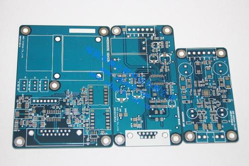
The guide hole alignment method uses the "guide hole" on the PCB to identify the number of layers of the PCB. The principle is mainly because the circuit connection of the multilayer PCB adopts the via technology. If we want to see how many layers the PCB has, we can identify it by looking at the vias.
On a basic PCB (single-sided motherboard), the parts are all concentrated on one side and the wires are all concentrated on the other side.
If you want to use a multi-layer board, you need to punch holes on the board so that the component pins can pass through the board to the other side, so the guide holes will penetrate the PCB board, so we can see that the pins of the part are soldered on the other side of.
For example, if the board uses a 4-layer board, then it needs to be routed on the 1st and 4th layers (signal layer), and the other layers have other uses (ground layer and power layer). Put the signal layer on the power layer and the power layer. The purpose of the two sides of the ground plane is to prevent mutual interference and facilitate modification of the signal lines.
If some board card guide holes appear on the front of the PCB, but cannot be found on the back, the EDA365 electronic forum believes that it must be a 6/8-layer board. If the same guide holes can be found on both sides of the PCB board, it is naturally a 4-layer board.
However, many board card manufacturers currently use another routing method, which is to connect only some of the lines, and use buried and blind via technologies in the routing. Blind via is to connect several layers of internal PCB to the surface PCB without penetrating the entire circuit board.
Buried vias are only connected to the internal PCB, so they cannot be seen from the surface only. Since the blind hole does not need to run through the entire PCB, if it is six layers or more, look at the board against the light source, and the light will not pass through. Therefore, there is a very popular saying before: the four-layer and six-layer or more PCBs are judged by whether the vias leak light or not.
This method has its reasons, and there are also inappropriate places. The EDA365 electronic forum believes that this method can only be used as a reference method.
Read recommendations:
Laminate copper-based PCB after 4L (sample)
Single-sided double-layer AL base PCB
Six-layer Immersion Gold Board (BGA)
Six-layer Immersion Gold Board (BGA)
Industrial Electronics PCB!What precautions should be taken when copying and grinding PCB boards
Popular recommended products
Six-layer Immersion Gold Board (BGA)
2021-05-24Display board (six layers)
2021-04-27Single copper base PCB
2021-04-27Six-layer Immersion Gold Board (BGA)
2021-05-27Aluminum substrate (double-sided)
2021-04-27Six-layer Immersion Gold Board (BGA)
2021-04-27High frequency PCB
2021-04-27High frequency PCB
2021-04-27Six-layer Immersion Gold Board (BGA)
2021-04-27Silver oil perforated plate (double-sided)
2021-04-27Six-layer Immersion Gold Board (BGA)
2021-04-27Six-layer Immersion Gold Board (BGA)
2021-05-27Six-layer Immersion Gold Board (BGA)
2021-04-27Mobile phone template (six layers)
2021-04-27Network communication board (sixth floor)
2021-04-29Six-layer Immersion Gold Board (BGA)
2021-05-27Six-layer Immersion Gold Board (BGA)
2021-05-24Laminate copper-based PCB after 4L (sample)
2021-04-27Single-sided double-layer AL base PCB
2021-04-27High frequency PCB
2021-04-27High frequency PCB
2021-04-27Computer card board (four layers)
2021-04-25Six-layer Immersion Gold Board (BGA)
2021-05-27Six-layer Immersion Gold Board (BGA)
2021-04-26Mobile phone board
2021-04-27Six-layer Immersion Gold Board (BGA)
2021-04-26SMT stickers
2021-05-27Six-layer Immersion Gold Board (BGA)
2021-04-26Six-layer Immersion Gold Board (BGA)
2021-04-26DIP plugin
2021-05-27DIP plugin
2021-05-27SMT stickers
2021-05-27Mobile phone board
2021-05-27Six-layer Immersion Gold Board (BGA)
2021-04-26Related Information
Composition of PCB
2024-09-29What is the difference between PCB and PCBA
2024-09-10PCB usage tips
2024-08-20Why do the circuit boards are green
2024-08-12How to clean the aluminum substrate?
2024-08-06Maintenance of Chemical Copper Plating Solution on PCB Board
2024-07-22single-sided PCB board and double-sided PCB board
2024-07-15PCB board production process flow
2024-07-09PCB CTI level
2024-07-01Via technology in circuit board factory.Automotive Electronics PCB
2024-06-25The role of FPC flexible circuit board solder mask
2024-06-18Detailed explanation of PCB board sampling production process
2024-06-11pcb v-cut depth standard
2024-05-27Multilayer Printed Circuit Board.What is the eq of PCB
2024-05-20The relationship between PCB safety distance and voltage
2024-04-22SMT surface mount processing.Hybrid circuit board PCB
2024-04-15PCB enterprises should pay attention to SMT matters.Electronic components PCB
2024-04-03PCB - the core building block of electronic products.Automotive Electronics PCB
2024-03-25PCB - the bridge and link of the electronic world
2024-03-18How to define high-frequency and high-precision circuit boards.Industrial Electronics PCB
2024-03-11USB PCB interface layout and wiring requirements
2024-01-22Electrolytic capacitor PCB.Steps for using PCB pins
2024-01-15Automotive ElectronicWhat aspects should be considered when processing and manufacturing PCB boards?
2024-01-08Electrolytic capaciWhat is the difference between a gold-plated circuit board and a gold-plated one?
2023-12-25When grinding PCB boards, attention should be paid to.Oscillator (belonging to crystal) PCB
2023-12-18Industrial Electronics PCB!What precautions should be taken when copying and grinding PCB boards
2023-12-11Do you know who is more suitable for LED direct display, regarding the difference between PCB board
2023-12-05Aluminum electrolytic capacitor PCB.What are the standards for selecting PCB boards
2023-11-27Surface Mount Technology (SMT) Phase PCB
2023-11-20Oscillator (belonging to crystal) PCB.The main functions of PCB board
2023-11-13