

source:Industry News release time:2023-02-20 Article author:yu Popular:pcb
The PCB board process can be roughly divided into the following two steps. Each process needs to be processed and produced in various processes. It should be noted that the processes of the boards of different structures are different. The following processes are the complete production process of multi -layer PCB process;
1. Inner layer; mainly to make the inner line of the PCB circuit board; the production process is:
1. Course: Cut the PCB substrate into production size;
2. Previous treatment: Clean the surface of the PCB substrate to remove surface pollutants
3, film compression: Paste the dry membrane on the surface of the PCB substrate to prepare for subsequent images;
4. Exposure: Use the exposure device to use UV light to expose the obtsession substrate, so as to transfer the image of the substrate to the dry membrane;
5. DE: The substrate will be exposed after exposure, which is displayed, etched, and removed, and the production of the inner plate will be completed
2. Internal inspection; mainly to detect and repair board lines;
1. AOI: AOI optical scanning, compares the image of the PCB board with the data of the good product that has been entered, so that the gaps and depression on the board image can be found;
2. VRS: The bad image data detected by AOI to VRS is passed to VRS, and relevant personnel are repaired.
3. Make up: welding the golden line on the gap or depression to prevent poor electrical;
CAD drawing PCB board circuit graph steps
A small circuit is of great significance. What is a circuit diagram? The designer of Dongguan Boyuan Electronics Co., Ltd. said that the circuit diagram was a circuit connection layout diagram of the component component composition and the relationship between them and the relationship between them from the needs of research or engineering planning.
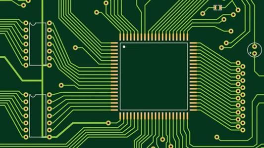
PCB diagram
However, the steps of CAD drawing PCB board circuit diagram are not complicated? The four major components of the circuit diagram of Boyuan Electronics are component symbols, connectivity, nodes, and annotations. The component symbol represents real circuit components, including resistors, capacitors, inductor coils, transistors, etc. Although graphics are not necessarily similar to actual components, they can generally highlight the characteristics of the component; Connected between several components or several wires.
The steps about the CAD PCB board circuit diagram include which are also the question of many new learners' associations. Below is the Boyuan Electronic designer to talk one by one.
In order to connect the convenient connection of the circuit system, the first thing is to learn the characteristics of the circuit. That is, based on this purpose, we must know the main use of the circuit diagram very clearly. Understand the principle of the role of the composition circuit, circuit equipment or circuit device; it provides a reference information for the failure of the test and finding the failure in the circuit system; and this will also be used as the basis for drawing the wiring diagram.
Read recommendations:
Network communication board (sixth floor)
Six-layer Immersion Gold Board (BGA)
The impact of pcb copper clad laminates on the upstream industry!Oscillator PCB factory
Popular recommended products
High frequency PCB
2021-04-27Mobile phone template (six layers)
2021-04-27Laminate copper-based PCB after 4L (sample)
2021-04-27Six-layer Immersion Gold Board (BGA)
2021-04-27High frequency PCB
2021-04-27Six-layer Immersion Gold Board (BGA)
2021-05-27Network communication board (sixth floor)
2021-04-29Display board (six layers)
2021-04-27High frequency PCB
2021-04-27Computer card board (four layers)
2021-04-25Six-layer Immersion Gold Board (BGA)
2021-05-24Six-layer Immersion Gold Board (BGA)
2021-05-27Single-sided double-layer AL base PCB
2021-04-27Six-layer Immersion Gold Board (BGA)
2021-04-27High frequency PCB
2021-04-27Six-layer Immersion Gold Board (BGA)
2021-05-27Silver oil perforated plate (double-sided)
2021-04-27Six-layer Immersion Gold Board (BGA)
2021-04-27Aluminum substrate (double-sided)
2021-04-27Six-layer Immersion Gold Board (BGA)
2021-05-24Single copper base PCB
2021-04-27Six-layer Immersion Gold Board (BGA)
2021-04-27Six-layer Immersion Gold Board (BGA)
2021-05-27SMT stickers
2021-05-27DIP plugin
2021-05-27Six-layer Immersion Gold Board (BGA)
2021-04-26Six-layer Immersion Gold Board (BGA)
2021-04-26Six-layer Immersion Gold Board (BGA)
2021-04-26Mobile phone board
2021-04-27DIP plugin
2021-05-27Mobile phone board
2021-05-27Six-layer Immersion Gold Board (BGA)
2021-04-26SMT stickers
2021-05-27Six-layer Immersion Gold Board (BGA)
2021-04-26Related Information
Composition of PCB
2024-09-29What is the difference between PCB and PCBA
2024-09-10PCB usage tips
2024-08-20Why do the circuit boards are green
2024-08-12How to clean the aluminum substrate?
2024-08-06Maintenance of Chemical Copper Plating Solution on PCB Board
2024-07-22single-sided PCB board and double-sided PCB board
2024-07-15PCB board production process flow
2024-07-09PCB CTI level
2024-07-01Via technology in circuit board factory.Automotive Electronics PCB
2024-06-25The role of FPC flexible circuit board solder mask
2024-06-18Detailed explanation of PCB board sampling production process
2024-06-11pcb v-cut depth standard
2024-05-27Multilayer Printed Circuit Board.What is the eq of PCB
2024-05-20The relationship between PCB safety distance and voltage
2024-04-22SMT surface mount processing.Hybrid circuit board PCB
2024-04-15PCB enterprises should pay attention to SMT matters.Electronic components PCB
2024-04-03PCB - the core building block of electronic products.Automotive Electronics PCB
2024-03-25PCB - the bridge and link of the electronic world
2024-03-18How to define high-frequency and high-precision circuit boards.Industrial Electronics PCB
2024-03-11USB PCB interface layout and wiring requirements
2024-01-22Electrolytic capacitor PCB.Steps for using PCB pins
2024-01-15Automotive ElectronicWhat aspects should be considered when processing and manufacturing PCB boards?
2024-01-08Electrolytic capaciWhat is the difference between a gold-plated circuit board and a gold-plated one?
2023-12-25When grinding PCB boards, attention should be paid to.Oscillator (belonging to crystal) PCB
2023-12-18Industrial Electronics PCB!What precautions should be taken when copying and grinding PCB boards
2023-12-11Do you know who is more suitable for LED direct display, regarding the difference between PCB board
2023-12-05Aluminum electrolytic capacitor PCB.What are the standards for selecting PCB boards
2023-11-27Surface Mount Technology (SMT) Phase PCB
2023-11-20Oscillator (belonging to crystal) PCB.The main functions of PCB board
2023-11-13
CopyRight © 2007-2025
粤ICP备2021061255号

Address:
1205, Floor 12, Building 3, Chuangyi Office Building, No. 110, Ziheng West Road, Jinsha Community, Kengzi Street, Pingshan District, Shenzhen, Guangdong, China

Tel:
+86-755-29662580

Email:
sales@victoriapcb.com

PCB

PCBA
Service
Process
 Tel: +86-755-29662580
 Email: sales@victoriapcb.com
 中
中 current position:


