source:Industry News release time:2022-11-21 Article author:yu Popular:pcb

① The wires used at the input and output terminals shall not be parallel to each other. It is better to add ground wire between lines to avoid feedback coupling.
② The minimum width of the printed circuit board conductor is mainly determined by the adhesion strength between the conductor and the insulating substrate and the current value flowing through them.
When the thickness of copper foil is 0.05 mm and the width is 1~15 mm, the temperature will not be higher than 3 ℃ when the current is 2 A, so the wire width of 1.5 mm can meet the requirements. For integrated circuits, especially digital circuits, 0.02-0.3 mm wire width is usually selected. Of course, as long as it is allowed, wide wires should be used as far as possible, especially power lines and ground wires.
The minimum spacing of wires is mainly determined by the insulation resistance and breakdown voltage between wires in the worst case. For integrated circuits, especially digital circuits, the spacing can be reduced to 5-8 um as long as the process allows.
③ The corners of printed wires are generally circular arcs, while right angles or included angles will affect the electrical performance in high-frequency circuits. In addition, avoid using large area copper foil as much as possible, otherwise, when heated for a long time, copper foil is easy to expand and fall off. When a large area of copper foil must be used, it is better to use grid shape, which is conducive to eliminating volatile gases generated by the heating of the adhesive between the copper foil and the substrate.
Pad
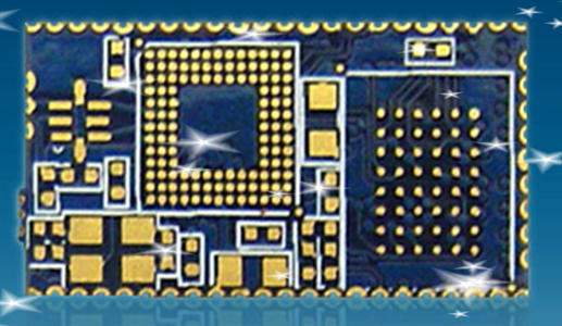
The center hole of the pad is slightly larger than the diameter of the device lead. If the pad is too large, it is easy to form faulty soldering. The outer diameter D of the pad is generally not less than d+1.2 mm, where d is the lead hole diameter. For high-density digital circuits, the minimum diameter of the pad can be d+1.0 mm
Read recommendations:
Silver oil perforated plate (double-sided)
Network communication board (sixth floor)
Six-layer Immersion Gold Board (BGA)
Popular recommended products
Six-layer Immersion Gold Board (BGA)
2021-05-27Six-layer Immersion Gold Board (BGA)
2021-05-27Mobile phone template (six layers)
2021-04-27Display board (six layers)
2021-04-27High frequency PCB
2021-04-27Six-layer Immersion Gold Board (BGA)
2021-05-24Computer card board (four layers)
2021-04-25Six-layer Immersion Gold Board (BGA)
2021-05-24Six-layer Immersion Gold Board (BGA)
2021-04-27Laminate copper-based PCB after 4L (sample)
2021-04-27Six-layer Immersion Gold Board (BGA)
2021-04-27High frequency PCB
2021-04-27High frequency PCB
2021-04-27Single copper base PCB
2021-04-27Single-sided double-layer AL base PCB
2021-04-27Six-layer Immersion Gold Board (BGA)
2021-05-27Six-layer Immersion Gold Board (BGA)
2021-04-27Aluminum substrate (double-sided)
2021-04-27Network communication board (sixth floor)
2021-04-29Six-layer Immersion Gold Board (BGA)
2021-05-27High frequency PCB
2021-04-27Silver oil perforated plate (double-sided)
2021-04-27Six-layer Immersion Gold Board (BGA)
2021-04-27Six-layer Immersion Gold Board (BGA)
2021-04-26SMT stickers
2021-05-27Six-layer Immersion Gold Board (BGA)
2021-04-26Mobile phone board
2021-04-27SMT stickers
2021-05-27Mobile phone board
2021-05-27Six-layer Immersion Gold Board (BGA)
2021-04-26Six-layer Immersion Gold Board (BGA)
2021-04-26DIP plugin
2021-05-27Six-layer Immersion Gold Board (BGA)
2021-04-26DIP plugin
2021-05-27Related Information
Composition of PCB
2024-09-29What is the difference between PCB and PCBA
2024-09-10PCB usage tips
2024-08-20Why do the circuit boards are green
2024-08-12How to clean the aluminum substrate?
2024-08-06Maintenance of Chemical Copper Plating Solution on PCB Board
2024-07-22single-sided PCB board and double-sided PCB board
2024-07-15PCB board production process flow
2024-07-09PCB CTI level
2024-07-01Via technology in circuit board factory.Automotive Electronics PCB
2024-06-25The role of FPC flexible circuit board solder mask
2024-06-18Detailed explanation of PCB board sampling production process
2024-06-11pcb v-cut depth standard
2024-05-27Multilayer Printed Circuit Board.What is the eq of PCB
2024-05-20The relationship between PCB safety distance and voltage
2024-04-22SMT surface mount processing.Hybrid circuit board PCB
2024-04-15PCB enterprises should pay attention to SMT matters.Electronic components PCB
2024-04-03PCB - the core building block of electronic products.Automotive Electronics PCB
2024-03-25PCB - the bridge and link of the electronic world
2024-03-18How to define high-frequency and high-precision circuit boards.Industrial Electronics PCB
2024-03-11USB PCB interface layout and wiring requirements
2024-01-22Electrolytic capacitor PCB.Steps for using PCB pins
2024-01-15Automotive ElectronicWhat aspects should be considered when processing and manufacturing PCB boards?
2024-01-08Electrolytic capaciWhat is the difference between a gold-plated circuit board and a gold-plated one?
2023-12-25When grinding PCB boards, attention should be paid to.Oscillator (belonging to crystal) PCB
2023-12-18Industrial Electronics PCB!What precautions should be taken when copying and grinding PCB boards
2023-12-11Do you know who is more suitable for LED direct display, regarding the difference between PCB board
2023-12-05Aluminum electrolytic capacitor PCB.What are the standards for selecting PCB boards
2023-11-27Surface Mount Technology (SMT) Phase PCB
2023-11-20Oscillator (belonging to crystal) PCB.The main functions of PCB board
2023-11-13