

source:Industry News release time:2021-11-26 Article author:sznbone Popular:pcb
What is the significance of PCB impedance to PCB circuit boards, and why do PCB circuit boards need impedance? This article first introduces what impedance and impedance types are. Secondly, it introduces why the PCB circuit board should be impedance. Finally, it explains the meaning of impedance to the PCB circuit board. Follow the editor to learn more about it.
In a circuit with resistance, inductance, and capacitance, the obstacle to alternating current is called impedance. Impedance is often represented by Z, which is a complex number. The real part is called resistance, and the imaginary part is called reactance. The hindering effect of capacitance on alternating current in the circuit is called capacitive reactance, and the hindering effect of inductance on alternating current in the circuit is called For inductive reactance, the obstructive effect of capacitance and inductance on alternating current in the circuit is collectively called reactance. The unit of impedance is ohms.
(1) Characteristic impedance
In electronic information products such as computers and wireless communications, the energy transmitted by the circuit board in the circuit is a square wave signal (square wave signal, called pulse) composed of voltage and time, and the resistance it encounters is called Is the characteristic impedance.
(2) Odd mode impedance
The impedance value of one line to ground of the two lines is the same as the impedance value of the two lines.
(3) Even mode impedance
Two identical signal waveforms with the same polarity are input to the drive end, and the impedance Zcom when the two wires are connected together.
(4) Differential impedance
Two identical signal waveforms with opposite polarities are input at the driving end, which are respectively transmitted by two differential lines, and the two differential signals are subtracted at the receiving end. The differential impedance is the impedance Zdiff between the two wires.
(5) Common mode impedance
The impedance Zoe of one line to the ground of the two lines is the same as the impedance value of the two lines, which is usually larger than the odd mode impedance.
The impedance of pcb circuit board refers to the parameters of resistance and reactance, which hinder the alternating current. In the production of pcb circuit boards, impedance processing is essential. The reasons are as follows:
1. The PCB circuit board (bottom of the board) should consider plugging and installing electronic components. After plugging, the conductivity and signal transmission performance should be considered. Therefore, the lower the impedance, the better, and the resistivity should be less than 1 per square centimeter.&TImes; Below 10-6.
2. During the production process, PCB circuit boards have to go through process steps such as copper sinking, tin electroplating (or chemical plating, or thermal spray tin), connector soldering, etc., and the materials used in these links must ensure that the resistivity is low, in order to ensure The overall impedance of the circuit board is low to meet the product quality requirements and can operate normally.
3. The tinning of PCB circuit boards is the most prone to problems in the entire circuit board production, and it is a key link that affects impedance. The biggest defect of the electroless tin coating is easy discoloration (easy to be oxidized or deliquescent) and poor solderability, which will lead to difficult soldering of the circuit board, high impedance, poor electrical conductivity, or instability of the overall board performance.
4. There are various signal transmissions in the conductors in the PCB circuit board. When it is necessary to increase its frequency in order to increase its transmission rate, if the circuit itself is different due to factors such as etching, stack thickness, wire width, etc., the impedance value will change. , So that its signal is distorted and the performance of the circuit board is degraded, so it is necessary to control the impedance value within a certain range.
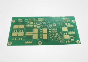
Impedance PCB circuit board diagram
Impedance PCB circuit board diagram
For the electronics industry, according to industry surveys, the most fatal weakness of the electroless tin coating is its easy discoloration (easy to be oxidized or deliquescent), poor brazing properties leading to difficult soldering, and high impedance leading to poor electrical conductivity or instability of the overall board performance. 、Easy long tin whiskers cause short circuit of PCB circuit and even burn out or catch fire.
It is reported that the first domestic research on chemical tin plating was Kunming University of Science and Technology in the early 1990s, followed by Guangzhou Tongqian Chemical (enterprise) in the late 1990s. Up to now, the industry has recognized that these two institutions are The best. Among them, according to our contact screening surveys, experimental observations and long-term endurance tests of many companies, it is confirmed that the tin-plated layer of Tongqian Chemical is a pure tin layer with low resistivity, and the quality of conductivity and brazing can be guaranteed to a high level. No wonder they dare to guarantee to the outside that the coating can keep its color for one year, no blistering, no peeling, and permanent tin whisker without any sealing and anti-tarnish protection.
Later, when the entire social production industry developed to a certain extent, many subsequent participants often copied each other. In fact, a considerable number of companies themselves did not have the R&D or initiative capabilities themselves. Therefore, many products and their users’ electronic products (circuit boards) The bottom of the board or the overall electronic product) performance is poor, and the main reason for the poor performance is the impedance problem, because when the unqualified electroless tin technology is in use, it is actually the tin plated on the PCB circuit board It is not really pure tin (or pure metal element), but tin compound (that is, it is not a metal element at all, but a metal compound, oxide or halide, or more directly a non-metal substance) or tin It is a mixture of compound and tin metal element, but it is difficult to find with the naked eye...
Because the main circuit of the PCB circuit board is copper foil, there is a tin-plated layer on the solder joints of the copper foil, and the electronic components are soldered on the tin-plated layer through solder paste (or solder wire). In fact, the solder paste is melting. The state soldered between the electronic component and the tin plating layer is metal tin (ie, a good conductive metal element), so you can simply point out that the electronic components are connected to the copper foil at the bottom of the circuit board through the tin plating layer, so the tin plating layer The purity and impedance of the instrument is the key; but before the electronic components are plugged in, when we directly use the instrument to detect the impedance, in fact, the two ends of the instrument probe (or called the test lead) first touch the copper foil on the bottom of the PCB board. The tin plating on the surface is then connected to the copper foil at the bottom of the PCB to communicate the current. Therefore, tin plating is the key, the key that affects the impedance and the key that affects the performance of the entire circuit board, and it is also the key that is easy to be ignored.
As we all know, except for the simple substance of metal, its compounds are poor electrical conductors or even non-conductive (also, this is the key to the distribution capacity or spreading capacity in the circuit), so there is this kind of quasi-conductive rather than conductive in the tin plating layer In the case of tin compounds or mixtures, the existing resistivity or the resistivity after the electrolysis reaction due to future oxidation or damp and the corresponding impedance are quite high (enough to affect the level or signal transmission in the digital circuit) and The characteristic impedance is also not consistent. So it will affect the performance of the circuit board and the whole machine.
Therefore, as far as the current social production phenomenon is concerned, the coating material and performance on the bottom of the circuit board are the most important and the most direct reason that affects the characteristic impedance of the entire circuit board. Because of its variability, the worrying impact of its impedance has become more invisible and changeable. The main reasons for its concealment are: firstly, it cannot be seen by the naked eye (including its changes), and secondly, it cannot be measured constantly because of its concealment. There is variability that changes with time and environmental humidity, so it is always easy to be ignored.
Read recommendations:
Six-layer Immersion Gold Board (BGA)
What is the use of car wireless charging of car wireless charging PCB?MCU PCB Collection
Popular recommended products
Six-layer Immersion Gold Board (BGA)
2021-04-27High frequency PCB
2021-04-27Six-layer Immersion Gold Board (BGA)
2021-05-27Six-layer Immersion Gold Board (BGA)
2021-04-27Six-layer Immersion Gold Board (BGA)
2021-05-27Single copper base PCB
2021-04-27Six-layer Immersion Gold Board (BGA)
2021-04-27High frequency PCB
2021-04-27Six-layer Immersion Gold Board (BGA)
2021-05-24Computer card board (four layers)
2021-04-25Single-sided double-layer AL base PCB
2021-04-27Six-layer Immersion Gold Board (BGA)
2021-05-24Aluminum substrate (double-sided)
2021-04-27Six-layer Immersion Gold Board (BGA)
2021-05-27Six-layer Immersion Gold Board (BGA)
2021-04-27High frequency PCB
2021-04-27Six-layer Immersion Gold Board (BGA)
2021-05-27Display board (six layers)
2021-04-27Network communication board (sixth floor)
2021-04-29Silver oil perforated plate (double-sided)
2021-04-27Mobile phone template (six layers)
2021-04-27Laminate copper-based PCB after 4L (sample)
2021-04-27High frequency PCB
2021-04-27Six-layer Immersion Gold Board (BGA)
2021-04-26DIP plugin
2021-05-27DIP plugin
2021-05-27Six-layer Immersion Gold Board (BGA)
2021-04-26Mobile phone board
2021-05-27SMT stickers
2021-05-27SMT stickers
2021-05-27Mobile phone board
2021-04-27Six-layer Immersion Gold Board (BGA)
2021-04-26Six-layer Immersion Gold Board (BGA)
2021-04-26Six-layer Immersion Gold Board (BGA)
2021-04-26Related Information
Composition of PCB
2024-09-29What is the difference between PCB and PCBA
2024-09-10PCB usage tips
2024-08-20Why do the circuit boards are green
2024-08-12How to clean the aluminum substrate?
2024-08-06Maintenance of Chemical Copper Plating Solution on PCB Board
2024-07-22single-sided PCB board and double-sided PCB board
2024-07-15PCB board production process flow
2024-07-09PCB CTI level
2024-07-01Via technology in circuit board factory.Automotive Electronics PCB
2024-06-25The role of FPC flexible circuit board solder mask
2024-06-18Detailed explanation of PCB board sampling production process
2024-06-11pcb v-cut depth standard
2024-05-27Multilayer Printed Circuit Board.What is the eq of PCB
2024-05-20The relationship between PCB safety distance and voltage
2024-04-22SMT surface mount processing.Hybrid circuit board PCB
2024-04-15PCB enterprises should pay attention to SMT matters.Electronic components PCB
2024-04-03PCB - the core building block of electronic products.Automotive Electronics PCB
2024-03-25PCB - the bridge and link of the electronic world
2024-03-18How to define high-frequency and high-precision circuit boards.Industrial Electronics PCB
2024-03-11USB PCB interface layout and wiring requirements
2024-01-22Electrolytic capacitor PCB.Steps for using PCB pins
2024-01-15Automotive ElectronicWhat aspects should be considered when processing and manufacturing PCB boards?
2024-01-08Electrolytic capaciWhat is the difference between a gold-plated circuit board and a gold-plated one?
2023-12-25When grinding PCB boards, attention should be paid to.Oscillator (belonging to crystal) PCB
2023-12-18Industrial Electronics PCB!What precautions should be taken when copying and grinding PCB boards
2023-12-11Do you know who is more suitable for LED direct display, regarding the difference between PCB board
2023-12-05Aluminum electrolytic capacitor PCB.What are the standards for selecting PCB boards
2023-11-27Surface Mount Technology (SMT) Phase PCB
2023-11-20Oscillator (belonging to crystal) PCB.The main functions of PCB board
2023-11-13
CopyRight © 2007-2025
粤ICP备2021061255号

Address:
1205, Floor 12, Building 3, Chuangyi Office Building, No. 110, Ziheng West Road, Jinsha Community, Kengzi Street, Pingshan District, Shenzhen, Guangdong, China

Tel:
+86-755-29662580

Email:
sales@victoriapcb.com

PCB

PCBA
Service
Process
 Tel: +86-755-29662580
 Email: sales@victoriapcb.com
 中
中 current position:


