

source:Industry News release time:2022-12-06 Article author:yu Popular:pcb
The problem of precision coincidence of multi-layer blind buried circuit boards
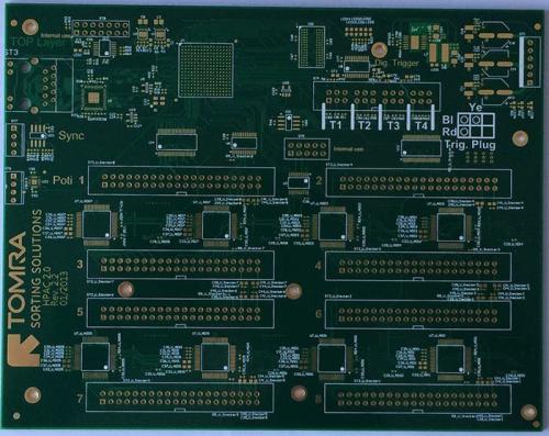
The printed circuit boards with multi-layer blind buried and blind via structures are generally completed by the "sub-board" production method, which means that it can only be completed after many times of pressing, drilling, hole plating, etc., so the precise positioning is very important.
High-precision printed circuit refers to the use of fine line width/spacing, tiny holes, narrow ring width (or no ring width), and buried and blind vias to achieve high density. And high precision means that the result of "thin, small, narrow, thin" will inevitably bring high precision requirements. Take the line width as an example: O.20mm line width, according to the regulations, the production of O.16-0.24mm is qualified, and its The error is (O.20±0.04)mm; and the line width of O.10mm, the same error is (0.10±O.02)mm, obviously the accuracy of the latter is doubled, and so on is not difficult to understand, The high precision requirements are therefore not discussed separately.
The combination technology of buried, blind and through-hole (multi-layer blind buried circuit board) is also an important way to improve the high density of printed circuits. Generally, buried and blind vias are tiny holes. In addition to increasing the number of wiring on the circuit board, buried and blind vias are interconnected between the "nearest" inner layers, which greatly reduces the number of through-holes formed, and the setting of isolation pads also will be greatly reduced, thereby increasing the number of effective wiring and interlayer interconnections in the board, and improving the high density of interconnections.
Coincidence between layers in the manufacture of multi-layer circuit boards with blind and buried holes
By adopting the pre-pin positioning system produced by ordinary multi-layer circuit boards, the pattern production of each layer and single piece is unified into one positioning system, which creates conditions for the success of manufacturing. For the ultra-thick single piece like the one used this time, if the thickness of the plate reaches 2 mm, the method of milling a certain thickness layer at the position of the positioning hole can also be classified into the processing of the punching four-slot positioning hole equipment of the front positioning system. in ability.
Read recommendations:
Computer card board (four layers)
Six-layer Immersion Gold Board (BGA)
Six-layer Immersion Gold Board (BGA)
How to reduce the risk of bending and deformation in PCB circuit board production?Inverter PCB Produ
Popular recommended products
Mobile phone template (six layers)
2021-04-27Six-layer Immersion Gold Board (BGA)
2021-04-27Aluminum substrate (double-sided)
2021-04-27Six-layer Immersion Gold Board (BGA)
2021-05-24High frequency PCB
2021-04-27Six-layer Immersion Gold Board (BGA)
2021-05-27High frequency PCB
2021-04-27Network communication board (sixth floor)
2021-04-29Six-layer Immersion Gold Board (BGA)
2021-04-27Single copper base PCB
2021-04-27Six-layer Immersion Gold Board (BGA)
2021-04-27High frequency PCB
2021-04-27Laminate copper-based PCB after 4L (sample)
2021-04-27Six-layer Immersion Gold Board (BGA)
2021-04-27High frequency PCB
2021-04-27Silver oil perforated plate (double-sided)
2021-04-27Computer card board (four layers)
2021-04-25Six-layer Immersion Gold Board (BGA)
2021-05-27Six-layer Immersion Gold Board (BGA)
2021-05-24Single-sided double-layer AL base PCB
2021-04-27Display board (six layers)
2021-04-27Six-layer Immersion Gold Board (BGA)
2021-05-27Six-layer Immersion Gold Board (BGA)
2021-05-27Six-layer Immersion Gold Board (BGA)
2021-04-26Six-layer Immersion Gold Board (BGA)
2021-04-26Mobile phone board
2021-04-27Six-layer Immersion Gold Board (BGA)
2021-04-26Six-layer Immersion Gold Board (BGA)
2021-04-26SMT stickers
2021-05-27DIP plugin
2021-05-27DIP plugin
2021-05-27Mobile phone board
2021-05-27Six-layer Immersion Gold Board (BGA)
2021-04-26SMT stickers
2021-05-27Related Information
Composition of PCB
2024-09-29What is the difference between PCB and PCBA
2024-09-10PCB usage tips
2024-08-20Why do the circuit boards are green
2024-08-12How to clean the aluminum substrate?
2024-08-06Maintenance of Chemical Copper Plating Solution on PCB Board
2024-07-22single-sided PCB board and double-sided PCB board
2024-07-15PCB board production process flow
2024-07-09PCB CTI level
2024-07-01Via technology in circuit board factory.Automotive Electronics PCB
2024-06-25The role of FPC flexible circuit board solder mask
2024-06-18Detailed explanation of PCB board sampling production process
2024-06-11pcb v-cut depth standard
2024-05-27Multilayer Printed Circuit Board.What is the eq of PCB
2024-05-20The relationship between PCB safety distance and voltage
2024-04-22SMT surface mount processing.Hybrid circuit board PCB
2024-04-15PCB enterprises should pay attention to SMT matters.Electronic components PCB
2024-04-03PCB - the core building block of electronic products.Automotive Electronics PCB
2024-03-25PCB - the bridge and link of the electronic world
2024-03-18How to define high-frequency and high-precision circuit boards.Industrial Electronics PCB
2024-03-11USB PCB interface layout and wiring requirements
2024-01-22Electrolytic capacitor PCB.Steps for using PCB pins
2024-01-15Automotive ElectronicWhat aspects should be considered when processing and manufacturing PCB boards?
2024-01-08Electrolytic capaciWhat is the difference between a gold-plated circuit board and a gold-plated one?
2023-12-25When grinding PCB boards, attention should be paid to.Oscillator (belonging to crystal) PCB
2023-12-18Industrial Electronics PCB!What precautions should be taken when copying and grinding PCB boards
2023-12-11Do you know who is more suitable for LED direct display, regarding the difference between PCB board
2023-12-05Aluminum electrolytic capacitor PCB.What are the standards for selecting PCB boards
2023-11-27Surface Mount Technology (SMT) Phase PCB
2023-11-20Oscillator (belonging to crystal) PCB.The main functions of PCB board
2023-11-13
CopyRight © 2007-2025
粤ICP备2021061255号

Address:
1205, Floor 12, Building 3, Chuangyi Office Building, No. 110, Ziheng West Road, Jinsha Community, Kengzi Street, Pingshan District, Shenzhen, Guangdong, China

Tel:
+86-755-29662580

Email:
sales@victoriapcb.com

PCB

PCBA
Service
Process
 Tel: +86-755-29662580
 Email: sales@victoriapcb.com
 中
中 current position:


