source:Industry News release time:2022-07-26 Article author:yu Popular:pcb

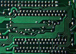
The poor tinning of the PCB board is generally related to the cleanliness of the surface of the PCB empty board. If there is no pollution, there will be basically no poor tinning. The second is the poor flux, temperature, etc. when tinning. Then the common electrical tin defects of printed circuit boards are mainly reflected in the following points:
1. There are particulate impurities in the plating layer of the pcb board, or there are polishing particles left on the surface of the circuit during the manufacturing process of the substrate.
2. The tin surface of the substrate or parts is oxidized and the copper surface is dark.
3. There are flakes on the pcb board that cannot be tinned, and there are particulate impurities in the plating on the board surface.
4. There are grease, impurities and other debris on the pcb board surface, or there is residual silicone oil.
5. The high-potential coating is rough, and there is a phenomenon of burning board. There are sheets on the PCB surface that cannot be tinned.
6. The coating on one side is complete, the coating on the other side is poor, and the low-potential hole has obvious bright edge phenomenon.
7. The edge of the low-potential hole has obvious bright edge phenomenon, the high-potential coating is rough, and there is a phenomenon of burning board.
8. Sufficient temperature or time is not guaranteed during the soldering process, or the flux is not used correctly.
9. The low-potential large area cannot be plated with tin, the surface of the board is slightly dark red or red, one side of the coating is complete, and the other side is poorly coated.
The reasons for poor tinning of pcb circuit boards are mainly reflected in the following points:
1. Too few anodes and uneven distribution.
2. Tin light agent is out of balance in small or excessive amounts.
3. There is some residual film or organic matter before plating.
4. The current density is too large and the plating solution is not filtered enough.
5. The composition of the bath potion is out of balance, the current density is too small, and the electroplating time is too short.
6. The anode is too long, the current density is too large, the local wire density of the pattern is too thin, and the light agent is out of balance.
Read recommendations:
Aluminum substrate (double-sided)
Computer card board (four layers)
Six-layer Immersion Gold Board (BGA)
What are the disadvantages of OSP anti-oxidation circuit board technology,X-ray inspection PCB price
Popular recommended products
High frequency PCB
2021-04-27Six-layer Immersion Gold Board (BGA)
2021-05-27Computer card board (four layers)
2021-04-25High frequency PCB
2021-04-27Six-layer Immersion Gold Board (BGA)
2021-05-27Mobile phone template (six layers)
2021-04-27Single-sided double-layer AL base PCB
2021-04-27Silver oil perforated plate (double-sided)
2021-04-27Six-layer Immersion Gold Board (BGA)
2021-04-27Six-layer Immersion Gold Board (BGA)
2021-05-27High frequency PCB
2021-04-27Display board (six layers)
2021-04-27Network communication board (sixth floor)
2021-04-29Six-layer Immersion Gold Board (BGA)
2021-04-27Six-layer Immersion Gold Board (BGA)
2021-05-27High frequency PCB
2021-04-27Aluminum substrate (double-sided)
2021-04-27Six-layer Immersion Gold Board (BGA)
2021-05-24Single copper base PCB
2021-04-27Six-layer Immersion Gold Board (BGA)
2021-05-24Laminate copper-based PCB after 4L (sample)
2021-04-27Six-layer Immersion Gold Board (BGA)
2021-04-27Six-layer Immersion Gold Board (BGA)
2021-04-27Six-layer Immersion Gold Board (BGA)
2021-04-26SMT stickers
2021-05-27DIP plugin
2021-05-27Six-layer Immersion Gold Board (BGA)
2021-04-26SMT stickers
2021-05-27Six-layer Immersion Gold Board (BGA)
2021-04-26Six-layer Immersion Gold Board (BGA)
2021-04-26Six-layer Immersion Gold Board (BGA)
2021-04-26Mobile phone board
2021-05-27Mobile phone board
2021-04-27DIP plugin
2021-05-27Related Information
Composition of PCB
2024-09-29What is the difference between PCB and PCBA
2024-09-10PCB usage tips
2024-08-20Why do the circuit boards are green
2024-08-12How to clean the aluminum substrate?
2024-08-06Maintenance of Chemical Copper Plating Solution on PCB Board
2024-07-22single-sided PCB board and double-sided PCB board
2024-07-15PCB board production process flow
2024-07-09PCB CTI level
2024-07-01Via technology in circuit board factory.Automotive Electronics PCB
2024-06-25The role of FPC flexible circuit board solder mask
2024-06-18Detailed explanation of PCB board sampling production process
2024-06-11pcb v-cut depth standard
2024-05-27Multilayer Printed Circuit Board.What is the eq of PCB
2024-05-20The relationship between PCB safety distance and voltage
2024-04-22SMT surface mount processing.Hybrid circuit board PCB
2024-04-15PCB enterprises should pay attention to SMT matters.Electronic components PCB
2024-04-03PCB - the core building block of electronic products.Automotive Electronics PCB
2024-03-25PCB - the bridge and link of the electronic world
2024-03-18How to define high-frequency and high-precision circuit boards.Industrial Electronics PCB
2024-03-11USB PCB interface layout and wiring requirements
2024-01-22Electrolytic capacitor PCB.Steps for using PCB pins
2024-01-15Automotive ElectronicWhat aspects should be considered when processing and manufacturing PCB boards?
2024-01-08Electrolytic capaciWhat is the difference between a gold-plated circuit board and a gold-plated one?
2023-12-25When grinding PCB boards, attention should be paid to.Oscillator (belonging to crystal) PCB
2023-12-18Industrial Electronics PCB!What precautions should be taken when copying and grinding PCB boards
2023-12-11Do you know who is more suitable for LED direct display, regarding the difference between PCB board
2023-12-05Aluminum electrolytic capacitor PCB.What are the standards for selecting PCB boards
2023-11-27Surface Mount Technology (SMT) Phase PCB
2023-11-20Oscillator (belonging to crystal) PCB.The main functions of PCB board
2023-11-13