source:Industry News release time:2023-07-27 Article author:yu Popular:pcb

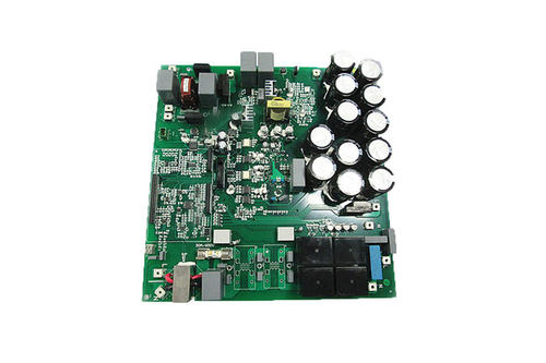
PCB design is a 'slow work leads to meticulous work' job, where everyone has their own set of solutions. Now let the engineer introduce to you what are the precautions for PCB design?
1. PCB design should have a reasonable direction
For example, input/output, AC/
DC, strong/weak signal, high/low frequency, high/low voltage, etc. Their directions should be linear (or separate) and cannot merge with each other. Its purpose is to prevent mutual interference.
2. Choosing a Good Contact Position in PCB Design
Usually, some commonality is required, such as the multiple grounding wires of the forward amplifier should converge and then be connected to the main line. In fact, due to various limitations, it is difficult to fully achieve this, but this principle should be followed as much as possible.
3. PCB design should correctly arrange capacitors
Usually only a few Line filter/Decoupling capacitor are drawn, but it is not indicated where they should be placed. In fact, these capacitors are designed for switchgear or other components that require filtering/decoupling, and they should be placed as close to these components as possible.
4. Appropriate size of buried holes and through-holes with required PCB design wire diameter requirements
The high-voltage and high-frequency lines should be slippery, without sharp corners or chamfers, and elbows should not be used at right angles; The ground should be as wide as possible, preferably using a large area of copper; The size of the pad or upper hole is too small, or the pad size does not match the drilling size correctly. The former is not suitable for manual drilling, while the latter is not suitable for CNC drilling, etc.
5. PCB design shall minimize the number of welding points and Linear density of each via
Some problems in the early stages of circuit board production are not easy to detect and often occur in the later stages, such as excessive wire holes and careless copper sinking process, which can lead to hidden dangers. Therefore, PCB design should minimize the number of upper scoring holes as much as possible.
Read recommendations:
Six-layer Immersion Gold Board (BGA)
Six-layer Immersion Gold Board (BGA)
Popular recommended products
Computer card board (four layers)
2021-04-25Six-layer Immersion Gold Board (BGA)
2021-05-27Aluminum substrate (double-sided)
2021-04-27Six-layer Immersion Gold Board (BGA)
2021-04-27Silver oil perforated plate (double-sided)
2021-04-27Single copper base PCB
2021-04-27High frequency PCB
2021-04-27Six-layer Immersion Gold Board (BGA)
2021-05-24Six-layer Immersion Gold Board (BGA)
2021-05-24Six-layer Immersion Gold Board (BGA)
2021-04-27Laminate copper-based PCB after 4L (sample)
2021-04-27Six-layer Immersion Gold Board (BGA)
2021-05-27Six-layer Immersion Gold Board (BGA)
2021-04-27Six-layer Immersion Gold Board (BGA)
2021-04-27High frequency PCB
2021-04-27Six-layer Immersion Gold Board (BGA)
2021-05-27Network communication board (sixth floor)
2021-04-29Mobile phone template (six layers)
2021-04-27High frequency PCB
2021-04-27Six-layer Immersion Gold Board (BGA)
2021-05-27Display board (six layers)
2021-04-27High frequency PCB
2021-04-27Single-sided double-layer AL base PCB
2021-04-27Six-layer Immersion Gold Board (BGA)
2021-04-26SMT stickers
2021-05-27DIP plugin
2021-05-27Mobile phone board
2021-04-27DIP plugin
2021-05-27Six-layer Immersion Gold Board (BGA)
2021-04-26Six-layer Immersion Gold Board (BGA)
2021-04-26Six-layer Immersion Gold Board (BGA)
2021-04-26Mobile phone board
2021-05-27SMT stickers
2021-05-27Six-layer Immersion Gold Board (BGA)
2021-04-26Related Information
Composition of PCB
2024-09-29What is the difference between PCB and PCBA
2024-09-10PCB usage tips
2024-08-20Why do the circuit boards are green
2024-08-12How to clean the aluminum substrate?
2024-08-06Maintenance of Chemical Copper Plating Solution on PCB Board
2024-07-22single-sided PCB board and double-sided PCB board
2024-07-15PCB board production process flow
2024-07-09PCB CTI level
2024-07-01Via technology in circuit board factory.Automotive Electronics PCB
2024-06-25The role of FPC flexible circuit board solder mask
2024-06-18Detailed explanation of PCB board sampling production process
2024-06-11pcb v-cut depth standard
2024-05-27Multilayer Printed Circuit Board.What is the eq of PCB
2024-05-20The relationship between PCB safety distance and voltage
2024-04-22SMT surface mount processing.Hybrid circuit board PCB
2024-04-15PCB enterprises should pay attention to SMT matters.Electronic components PCB
2024-04-03PCB - the core building block of electronic products.Automotive Electronics PCB
2024-03-25PCB - the bridge and link of the electronic world
2024-03-18How to define high-frequency and high-precision circuit boards.Industrial Electronics PCB
2024-03-11USB PCB interface layout and wiring requirements
2024-01-22Electrolytic capacitor PCB.Steps for using PCB pins
2024-01-15Automotive ElectronicWhat aspects should be considered when processing and manufacturing PCB boards?
2024-01-08Electrolytic capaciWhat is the difference between a gold-plated circuit board and a gold-plated one?
2023-12-25When grinding PCB boards, attention should be paid to.Oscillator (belonging to crystal) PCB
2023-12-18Industrial Electronics PCB!What precautions should be taken when copying and grinding PCB boards
2023-12-11Do you know who is more suitable for LED direct display, regarding the difference between PCB board
2023-12-05Aluminum electrolytic capacitor PCB.What are the standards for selecting PCB boards
2023-11-27Surface Mount Technology (SMT) Phase PCB
2023-11-20Oscillator (belonging to crystal) PCB.The main functions of PCB board
2023-11-13